


162
CHAPTER 4 BUS INTERFACE
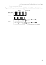
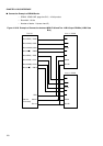
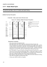
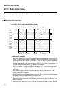
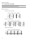
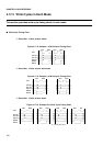
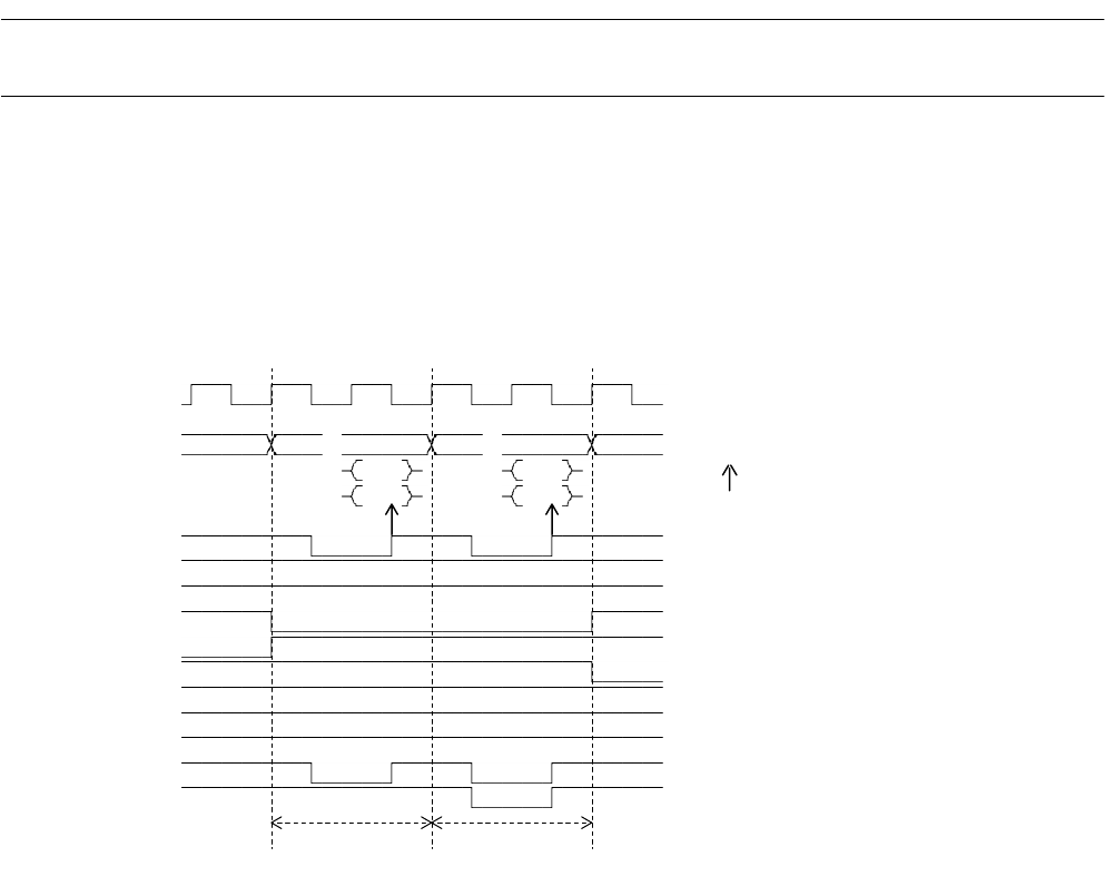
4.17.1 Basic Read Cycle
This section provides a chart of the basic read cycle timing.
■
Basic Read Cycle Timing Chart
❍
Bus width: 16 bits, access: words, CS0 area access
Figure 4.17-1 Example of Basic Read Cycle Timing Chart
[Explanation of operation]
• CLK outputs external bus operation clocks.
When gear control is set, the CLK frequency is lowered according to the gear ratio.
• A24 to A00 (address 24 to address 00) output the address of the first byte location, specified
in word, half-word, or byte access in read cycles, from the beginning (BA1) of bus cycles. In
the above example, word access is performed in a 16-bit bus width. Therefore, the address
(lower 2 bits: "0") of the upper 16 bits in the word access is output in the first bus cycle, and
the address (lower 2 bits: "2") of the lower 16 bits is output in the second bus cycle.
• D31 to D16 (data 31 to data 16) represent read data from external memory and I/O. In read
cycles, D31 to D16 are read at the rising edge of RDX. In read cycles, all data from D31 to
D16 is read at the rising edge of RDX, regardless of the bus width and word, half-word, and
byte access. Whether the fetched data is valid is determined inside the chip.
• RDX represents read strobe signals on the external data bus that are asserted at the falling
edge of BA1 and negated at the falling edge of BA2.
• In read cycles, WR0X and WR1X are negated.
BA1 BA2 BA1 BA2
CLK
A24-00 #0 #2
D31-24 #0 #2
D23-16 #1 #3
RDX
WR0X
WR1X
CS0X
CS1X
CS2X
CS3X
CS4X
CS5X
(DACK0)
(EOP0)
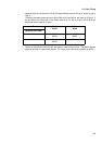
- # of A24-00 represents the lower 2 bits
- # of D31-16 represents read data byte
- represents read data fetch times.
- (DACK0) and (E0P0) represent DMAC
Half-word access
side
addresses.
bus cycles.
of upper address
side
Half-word access
of lower address
of an address.