


95
3.10 Standby Mode (Low Power Consumption Mechanism)
3.10.2 Sleep State
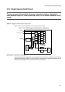
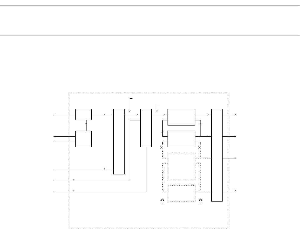
This section provides information on transition to the sleep state and returning from
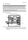
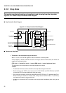
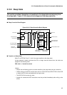
the sleep state. Figure 3.10.2 shows a block diagram of the sleep controller.
■
Sleep Controller Block Diagram
Figure 3.10-2 Sleep Controller Block Diagram
■
Transition to Sleep State
Write "0" to STCR bit 7 and "1" to bit 6 to cause transition to the sleep state.
A sleep request is issued, and when the CPU no longer uses the internal bus, the clocks are
stopped in the following order:
CPU clock --> internal bus clock
<Notes>
• Always use the following routine to cause transition to the sleep state using an instruction.
• Before writing to the STCR, set the same value in CCK1/CCK0 and PCK1/PCK0 of the GCR
to match the CPU clock and peripheral clock gear ratios.
• The GCR CHC bit can be any value.
• At least six consecutive NOP instructions must be provided immediately after writing to the
STCR.
STCR
SLEP
clear
.or.
Internal bus
Internal interrupt
Internal reset
CPU hold enabled
CPU hold request
Sleep state
indication signal
State transition control circuit
Sleep state transition request signal
Stop signal
State decoder
CPU clock
generation
Internal
bus clock
generation
Internal
DMA clock
generation
External
bus clock
generation
Internal
peripheral
clock
generation
Clock stop
request signal
Clock release
request signal
Internal clock generation circuit
CPU clock
Internal bus clock
Internal DMA clock
External bus clock
Internal peripheral clock