


20
CHAPTER 1 OVERVIEW
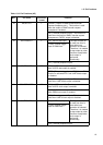
83 SO1/TRG3/PF4 F [SO1] UART1 data output. This function is valid
when UART1 data output is enabled.
[TRG3] External trigger input of PWM timer. This
function is valid when PF4 and UART1 data output
is disabled.
[PF4] General-purpose I/O port. This function is
valid when UART1 data output is disabled.
Table 1.5-4 Pin Functions (4/5)
NO. Pin name I/O circuit
format
Function
Table 1.5-5 Pin Functions (5/5)
NO. Pin name I/O circuit
format
Function
84 SI2/OCPA1/PF5 F [SI2] UART2 data input This input is used from
time to time while UART2 is operating for input.
Therefore, it is needed to stop output by other
functions except when such output is performed
intentionally.
[OCPA1] PWM timer output. This function is valid
when PWM timer output is enabled.
[PF5] General-purpose I/O port.
85 SO2/OCPA2/PF6 F [SO2] UART2 data output. This function is valid
when UART2 data output is enabled.
[OCPA2] PWM timer output. This function is valid
when PWM timer output is enabled.
[PF6] General-purpose I/O port. This function is
valid when UART2 data output is disabled.
86 OCPA0/PF7/ATGX F [OCPA0] PWM timer output. This function is valid
when PWM timer output is enabled.
[PF7] General-purpose I/O port. This function is
valid when PWM timer output is disabled.
[ATGX] External trigger input for A/D converter.
This input is used from time to time when this pin is
selected for the A/D start cause. Therefore, it is
needed to stop output by other functions except
when such output is performed intentionally.
87
to
90
AN0 to AN3 G [AN0-3] A/D converter analog input.
91 AVCC - VCC power supply for A/D converter