


129
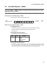
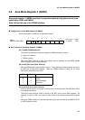
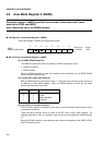
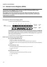
4.10 DRAM Control Register 4/5 (DMCR4/5)
[bit 4] REFE (REFresh Enable bit)
The REFE bit specifies whether to perform the cyclic refresh operation of the CAS before
RAS (CBR) type. When starting the cyclic refresh, regardless of areas 4 and 5, set the
REFE bit of DMCR4 or DMCR5 to "1" and set the STR bit of the refresh control register
(RFCF).
0: Does not perform a cyclic refresh (initial value).
1: Performs cyclic refresh with an interval specified by the refresh control register (RFCR).
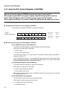
[bit 3] PAR (PARity select bit)
This device supports no parity function.
Setting this bit has no effect.
[bit 2] PERR (Parity ERRor bit)
This device supports no parity function.
Setting this bit has no effect.
[bit 1] PEIE (Parity Error Interrupt Enable bit)
The PEIE bit specifies whether to output an interrupt request for a parity error.
This device supports no parity function.
Be sure to set this bit to "0".
■
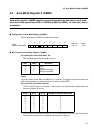
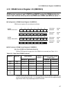
Bus Width Combinations
Table 4.10.2 lists the combinations of bus widths available in areas 4 and 5.
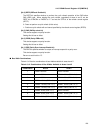
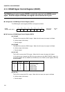
Table 4.10-2 Combinations of Bus Widths Available in Areas 4 and 5
Combination Area 4 Area 5
1 Usual: 16/8 bits Usual: 16/8 bits
2 Usual: 16/8 bits DRAM: 16 bits (C/W = 0, 1)
3 Usual: 16/8 bits DRAM: 8 bits (C/W = 0, 1)
4 DRAM: 16 bits (C/W = 0, 1) Usual: 16/8 bits
5 DRAM: 16 bits (C/W = 0, 1) DRAM: 16 bits (C/W = 0, 1)
6 DRAM: 16 bits (C/W = 0, 1) DRAM: 8 bits (C/W = 0, 1)
7 DRAM: 8 bits (C/W = 0, 1) Usual: 16/8 bits
8 DRAM: 8 bits (C/W = 0, 1) DRAM: 16 bits (C/W = 0, 1)
9 DRAM: 8 bits (C/W = 0, 1) DRAM: 8 bits (C/W = 0, 1)