


164
CHAPTER 4 BUS INTERFACE
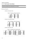
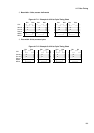
4.17.2 Basic Write Cycles
This section provides a chart of the basic write cycle timing.
■
Basic Write Cycle Timing Chart
❍
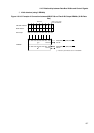
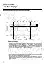
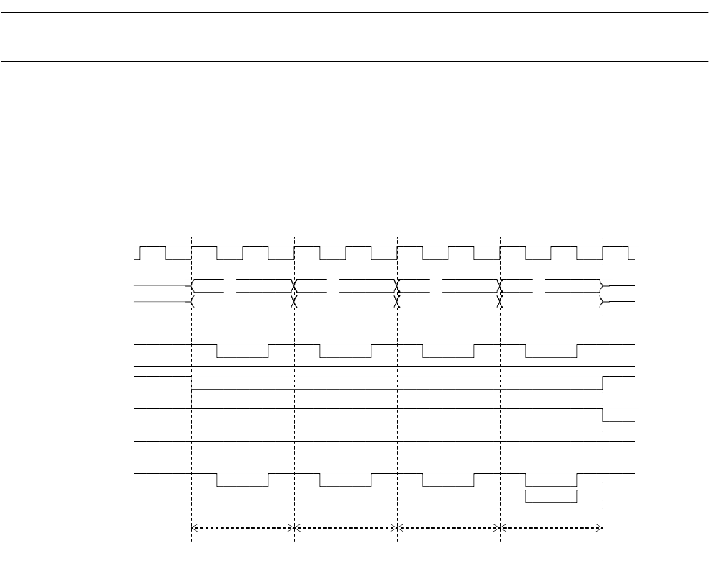
Bus width: 8 bits, access: words, CS0 area access
Figure 4.17-2 Example for Basic Write Cycle Timing
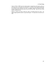
[Explanation of operation]
• A24 to A00 (address 24 to address 00) output the address of the first byte location, specified
in word, half-word, or byte access in write cycles, from the beginning (BA1) of bus cycles. In
the above example, word access is performed in an 8-bit bus width. Therefore, the address
of the first byte (the lower side of the address: "0") in the word access is first output. The
following three addresses are then sequentially output: "1" (+1 byte from the first byte), "2"
(+2 bytes from the first byte), and "3" (+3 bytes from the first byte).
• D31 to D16 (data 31 to data 16) represent write data to I/O. In write cycles, write data is
output from the beginning (BA1) of bus cycles and set to High-Z at the end (end of BA2) of
bus cycles.
As the above example has an 8-bit data bus width, write data is output from D31 to D24.
• In write cycles, RDX is negated.
• WR0X and WR1X are write strobe signals on the external data bus that are asserted at the
falling edge of BA1 and negated at the falling edge of BA2.
D31 to D24 and D23 to D16 are asserted, depending on the corresponding data buses,
WR0X and WR1X, respectively. As the above example has an 8-bit data bus width, only
WR0X is asserted.
• When chip select areas 0 to 5 have a maximum bus width of 8 bits, that is, when all of the
BA1 BA2 BA1 BA2 BA1 BA2 BA1 BA2
CLK
A24-00 #0 #1 #2 #3
D31-24 #0 #1 #2 #3
D23-16
RDX
WR0X
WR1X
CS0X
CS1X
CS2X
CS3X
CS4X
CS5X
(DACK0)
(EOP0)
Byte access to
address '0' at the
lower 2bits
Byte access to
address '1' at the
lower 2bits
Byte access to
address '2' at the
lower 2bits
Byte access to
address '3' at the
lower 2bits