


173
4.17 Bus Timing
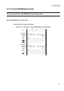
4.17.8 Usual DRAM Interface: Read
This section provides a usual DRAM interface read timing chart.
■
Usual DRAM Interface: Read Timing Chart
❍
Bus width: 16 bits, access: words, CS4 area access
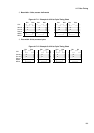
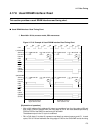
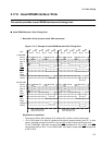
Figure 4.17-16 Example of Usual DRAM Interface Read Timing Chart
[Explanation of operation]
• A24 to A00 (address 24 to address 00) output a row address from the rising edge of Q2 and
then output a column address from the rising edge of Q4 for the read address specified by
PGS3 to PGS0 of the DMCR as well as by the bus width.
The address output in the Q1 cycle is undefined.
• D31 to D16 (data 31 to data 16) represent read data from external memory and I/O. In read
cycles, D31 to D16 are fetched at the rising edge of CAS for the 1CAS/2WE and at the rising
Q1 Q2 Q3 Q4 Q5 Q1 Q2 Q3 Q4 Q5
CLK
1)1CAS/2WE
A24-00
X #0 row.adr. #0 col.adr X #2 row.adr. #2 col.adr
D31-24 #0 #2
D23-16 #1 #3
RAS
CAS
WEL
WEH
RDX
CS4X
(DACK0)
(EOP0)
2)2CAS/1WE
A24-00
X #0 row.adr. #0 col.adr X #2 row.adr. #2 col.adr
D31-24 #0 #2
D23-16 #1 #3
RAS
CASL
CASH
WE
RDX
CS4X
(DACK0)
(EOP0)
Half-word access of Half-word access of
upper address side lower address side