191
4.17 Bus Timing
4.17.20 DRAM Refresh
This section provides DRAM refresh timing charts.
■
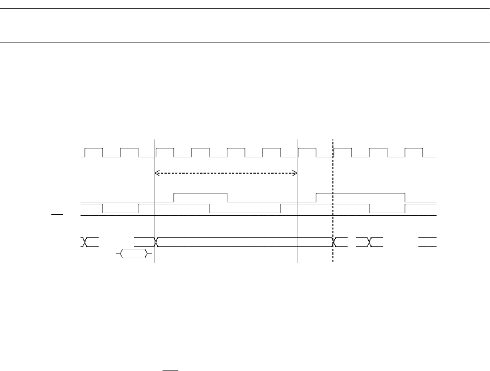
CAS before RAS (CBR) Refresh
Figure 4.17-35 Example of CAS before RAS (CBR) Refresh Timing Chart
[Explanation of operation]
• When executing CBR refresh, set the REFE bit of DMCR4 and DMCR5 and the STR bit of
the RFCR.
• This manual represent the CBR cycle by R1 to R4.
CAS is asserted at the falling edge of the R2 cycle and negated at the falling edge of the R4
cycle.
RAS is asserted at the rising edge of the R3 cycle and negated at the falling edge of the idle
cycle next to R4. WE
is negated in the CBR cycle.
• For the 1CAS/2WE, CAS is output ; for the 2CAS/1WE, both CASL and CASH are output at
the time describe above.
• The priority of CRB refresh is higher than that of DRAM bus access.
During DRAM access, for example, during word access in an 8-bit bus width, four times of
bus access are required. In this case, even if a refresh request is detected from the first to
third bus access, the refresh is not executed until the fourth bus cycle ends.
CBR refresh is always executed when the last access cycle ends.
• DRAM access at the end of CBR refresh always starts from the Q1 cycle that indicates the
start of that access, and data output starts with the row address even if the next bus access
is within a page.
• CBR refresh is executed periodically even under the following conditions:
• Usual bus access other DRAM access is performed.
• The external bus is released (BGRNTX is "L").
• The CPU is sleeping.
Q4 Q5 R1 R2 R3 R4 idle Q1 Q2 Q3
CLK
CBR
RAS
CAS
WE
A24-00 col.adr. xx row.adr.
D31-16


