185
4.17 Bus Timing
4.17.14 Single DRAM Interface: Read
This section provides a read timing chart for a single DRAM interface.
■
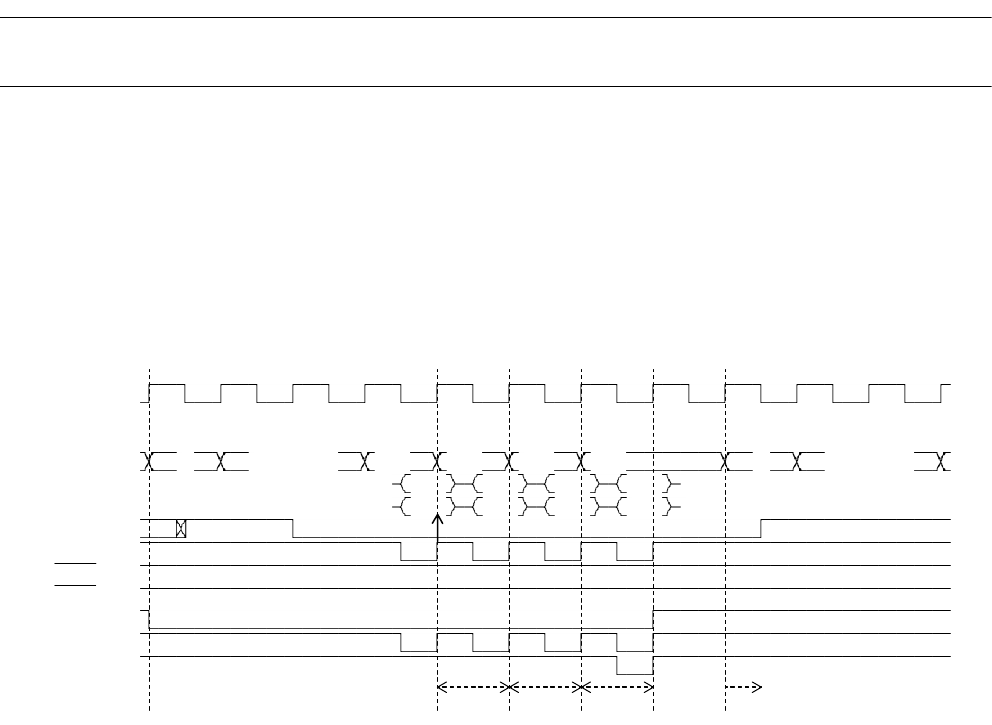
Single DRAM Interface: Read Timing Chart
❍
Bus width: 16 bits, access: words
Figure 4.17-29 Example of Single DRAM Interface Read Timing Chart
[Explanation of operation]
• Column addresses are output in Q4SR cycles.
• CAS is asserted at the falling edge of Q4SR
• D31 to D16 are fetched at the rising edge of CAS (including CASL and CASH) as in the case
of the usual DRAM interface.
• When a read cycle ends, at least one idle clock cycle is inserted so as to prevent conflicts
between the external data buses.
• DACK0 to DACK2 and E0P0 to E002 are output at the same time as CAS.
Q1 Q2 Q3 Q4SR Q4SR Q4SR Q4SR Q1 Q2 Q3
CLK
1)1CAS/2WE
A24-00
X row.adr. col. col. col. col. X row.adr.
D31-24
D23-16
RAS
CAS
WEL
WEH
RDX
(DACK0)
(EOP0)
Outside of page
Read
Read
Read
Read
Idle
Read
Read
Read
Read
High speed
page
High speed
page
High speed
page


