188
CHAPTER 4 BUS INTERFACE
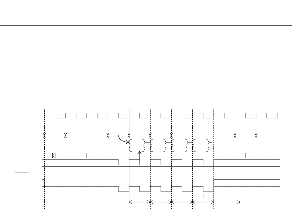
4.17.17 Hyper DRAM Interface: Read
This section provides a hyper DRAM interface timing chart.
■
Hyper DRAM Interface: Read Timing Chart
❍
Bus width: 16 bits, access: words
Figure 4.17-32 Example of Hyper DRAM Interface Read Timing Chart
[Explanation of operation]
• Column addresses are output in Q4HR cycles.
• CAS is asserted at the falling edge of Q4HR and negated at the rising edge of Q4HR.
• D31 to D16 are fetched at the falling edge of CAS to be output in the Q4HR cycle next to that
in which the corresponding column address is output.
• After a read cycle ends, at least one idle clock cycle is inserted so as to prevent conflicts
between the external data buses.
• DACK0 to DACK2 and E0P0 to E0P2 are output at the same time as CAS.
Q1 Q2 Q3 Q4HR Q4HR Q4HR Q4HR Q4HR Q1 Q3
CLK
1CAS/2WE
A24-00
X row.adr. col.0 col.2 col.4 col.6 X row.a
D31-24
D23-16
RAS
CAS
WEL
WEH
RDX
(DACK0)
(EOP0)
Outside page
1)
Read1
Read0
Idle
Read3
Read2
Read5
Read4
Read7
Read6
High
speed
page
High
speed
page
High
speed
page
High
speed
page


