


14
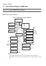
CHAPTER 1 OVERVIEW
1.5 Pin Functions
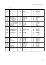
Tables 1.5.1 to 1.5.5 lists the MB91F109 pin functions.
The numbers shown in the tables has nothing to do with the package pin numbers.
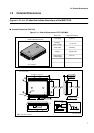
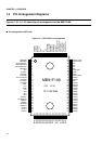
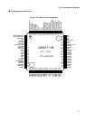
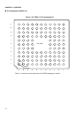
Since pins have different pin numbers among QFP, LQFP, and FBGA, see Section 1.4,
"Pin Arrangement Diagrams."
■
Pin Functions
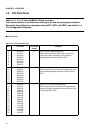
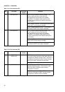
Table 1.5-1 Pin Functions (1/5)
NO. Pin name I/O circuit
format
Function
1
2
3
4
5
6
7
8
D16/P20
D17/P21
D18/P22
D19/P23
D20/P24
D21/P25
D22/P26
D23/P27
E Bits 16 to 23 of external data bus.
When the external bus width is set to 8 bits or in
single-chip mode, these pins can be used as
general-purpose I/O ports (P20 to P27).
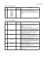
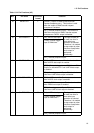
9
10
11
12
13
14
15
16
D24/P30
D25/P31
D26/P32
D27/P33
D28/P34
D29/P35
D30/P36
D31/P37
E Bits 24 to 31 of external data bus.
When these pins are not used for the data bus, they
can be used as general-purpose I/O ports (P30 to
P37).
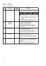
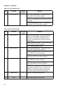
17
18
19
20
21
22
23
24
25
26
27
28
29
30
31
32
A00/P40
A01/P41
A02/P52
A03/P43
A04/P44
A05/P45
A06/P46
A07/P47
A08/P50
A09/P51
A10/P52
A11/P53
A12/P54
A13/P55
A14/P56
A15/P57
F Bits 00 to 15 of external address bus.
When these pins are not used for the address bus,
they can be used as general-purpose I/O ports (P40
to P47 and P50 to P57).