


175
4.17 Bus Timing
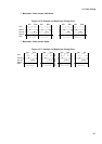
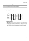
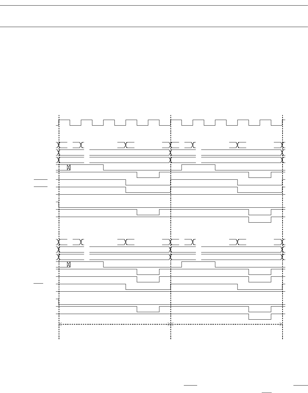
4.17.9 Usual DRAM Interface: Write
This section provides a usual DRAM interface write timing chart.
■
Usual DRAM Interface: Write Timing Chart
❍
Bus width: 16 bits, access: words, CS4 area access
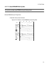
Figure 4.17-17 Example of Usual DRAM Interface Write Timing Chart
[Explanation of operation]
• The output of A24 to A00 (address 24 to address 00) is similar to that at read cycles.
• D31 to D16 (data 31 to data 16) represent write data to external memory and I/O. In write
cycles, write data is output from the Q1 cycle and set to High-Z when the Q5 cycle ends.
For the 1CAS/2WE, valid data is output while WEL
corresponds to D31 to D24, and WEH
corresponds toD23 to D16. For the 2CAS/1WE, valid data is output while WE corresponds
to D31 to D16.
Q1
CLK
X #0 row.adr. #0 col.adr X #2 row.adr. #2 col.adr
D31-24 #0 #2
D23-16 #1 #3
RAS
CAS
WEL
WEH
RDX
CS4X
(DACK0)
(EOP0)
X #0 row.adr. #0 col.adr X #2 row.adr. #2 col.adr
D31-24 #0 #2
D23-16 #1 #3
RAS
CASL
CASH
WE
RDX
CS4X
(DACK0)
(EOP0)
Q2 Q3 Q4 Q5 Q1 Q2 Q3 Q4 Q5
A24-00
A24-00
Half-word access of Half-word access of
upper address side lower address side
1)1CAS/2WE
2)2CAS/1WE