114
CHAPTER 4 BUS INTERFACE
■
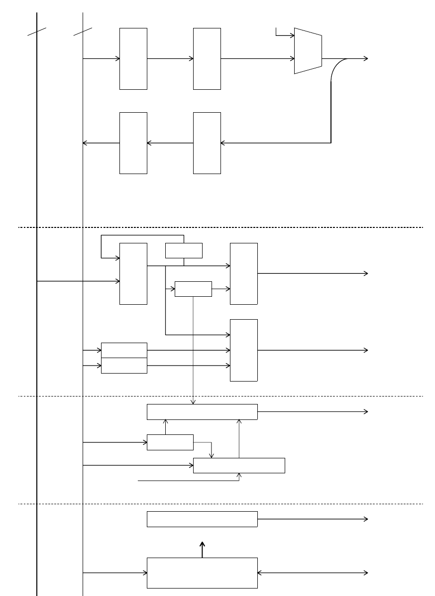
Block Diagram of the Bus Interface
Figure 4.1.2 shows a block diagram of the bus interface
Figure 4.1-2 Bus Interface Block Diagram
32 32 A-OUT
EXTERNAL
DATA B US
MUX
write buffer switch
read buffer switch
DATA BLOCK
ADDRESS BLOCK
+1or+2
EXTERNAL
ADDRESS BUS
inpage
address buffer shifter
ASR CS0X-CS5X
AMR
comparator
DRAM control RAS0,RAS1
CS0L,CS1L
CS0H,CS1H
underflow DW0X,DW1X
DMCR
refresh counter
from TBT
RDX
WR0X,WR1X
BRQ
registers BGRNTX
& CLK
control RDY
ADDRESS BUS DATA BUS
External pin control block
Control of all blocks


