


181
4.17 Bus Timing
4.17.12 Automatic Wait Cycles in Usual DRAM Interface
This section provides an automatic wait cycle timing chart in the usual DRAM
interface.
■
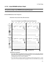
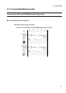
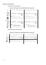
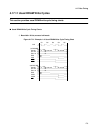
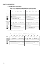
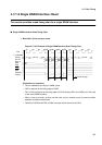
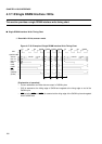
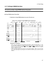
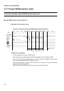
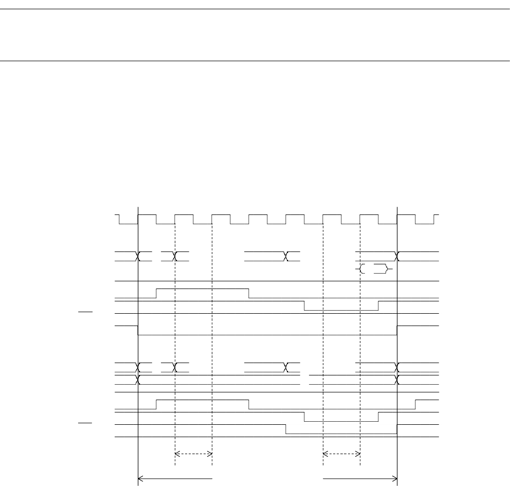
Automatic Wait Cycle Timing Chart in Usual DRAM Interface
❍
Bus width: 8 bits, access: bytes
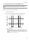
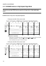
Figure 4.17-24 Example of Automatic Wait Cycle Timing Chart in Usual DRAM Interface
[Explanation of operation]
• When adding only one wait clock cycle to the Q1 and Q4 cycles, set the Q1W and Q4W bits
of DMCR4 and DMCR5. The inserted cycles are called the "Q1W" and "Q4W" cycles.
The Q1W and Q4W cycles execute the same cycles as the Q1 and Q4 cycles. By this
operation, the "H" width of RAS and the "L" width of CAS can be extended by one cycle,
respectively.
Set the widths according to the DRAM access time.
Q1 Q1W Q2 Q3 Q4 Q4W Q5
CLK
1)Read
A24-00
X #0 row.adr. #0 col.adr.
D31-24 #0
D23-16
RAS
CAS
WE
RDX
2)Write
A24-00
X #0 row.adr. #0 col.adr.
D31-24 #0
D23-16
RAS
CAS
WE
RDX
Q1 wait Q4 wait
Usual DRAM interface