


75
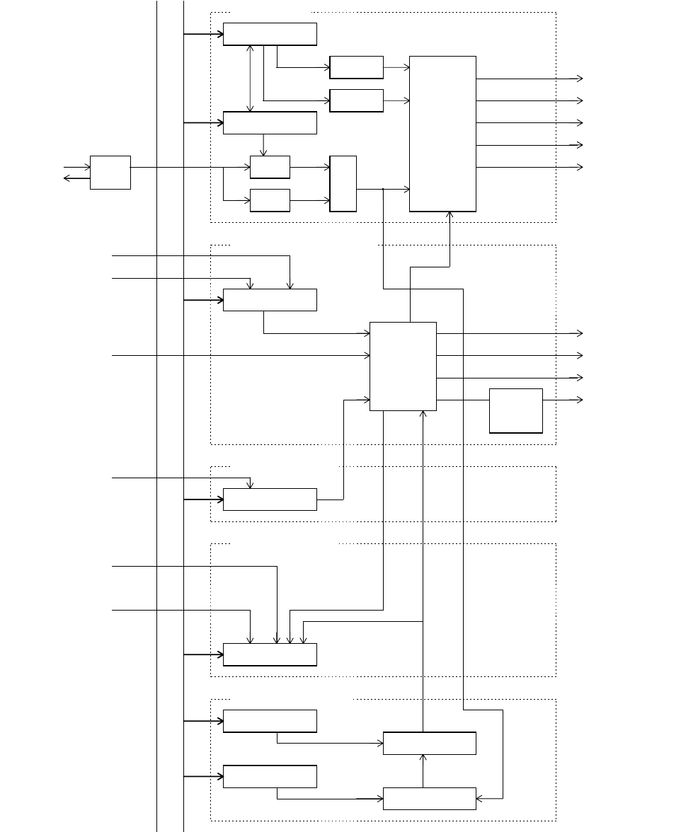
3.1 Outline of Clock Generator and Controller
■
Clock Generator and Controller Block Diagram
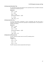
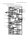
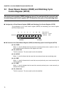
Figure 3.1.2 is a block diagram of the clock generator and controller.
Figure 3.1-2 Block Diagram of the Clock Generator and Controller
X0 PLL
X1
1/2
R
|
B
U
S
[Gear controller]
GCR register
CPU gear
Peripheral
gear
PCTR register
Oscilla-
tion
circuit
Selector
circuit
Internal
clock
generation
circuit
CPU clock
Internal bus clock
External bus clock
Peripheral
DMA clock
Internal peripheral
clock
[Stop/sleep controller]
Internal interrupt
Internal reset
STCR register
CPU hold permission
Status
transition
control
circuit
Stop state
Sleep state
CPU hold request
Internal reset
Reset
generation
F/F
[DMA suppression
circuit]
DMA request
PDRR register
[Reset reason circuit]
Power-on reset
RSTX pin
RSRR register
[Watchdog controller]
WPR register
Watchdog F/F
CTBR register
Timebase timer
Count clock