189
4.17 Bus Timing
4.17.18 Hyper DRAM Interface: Write
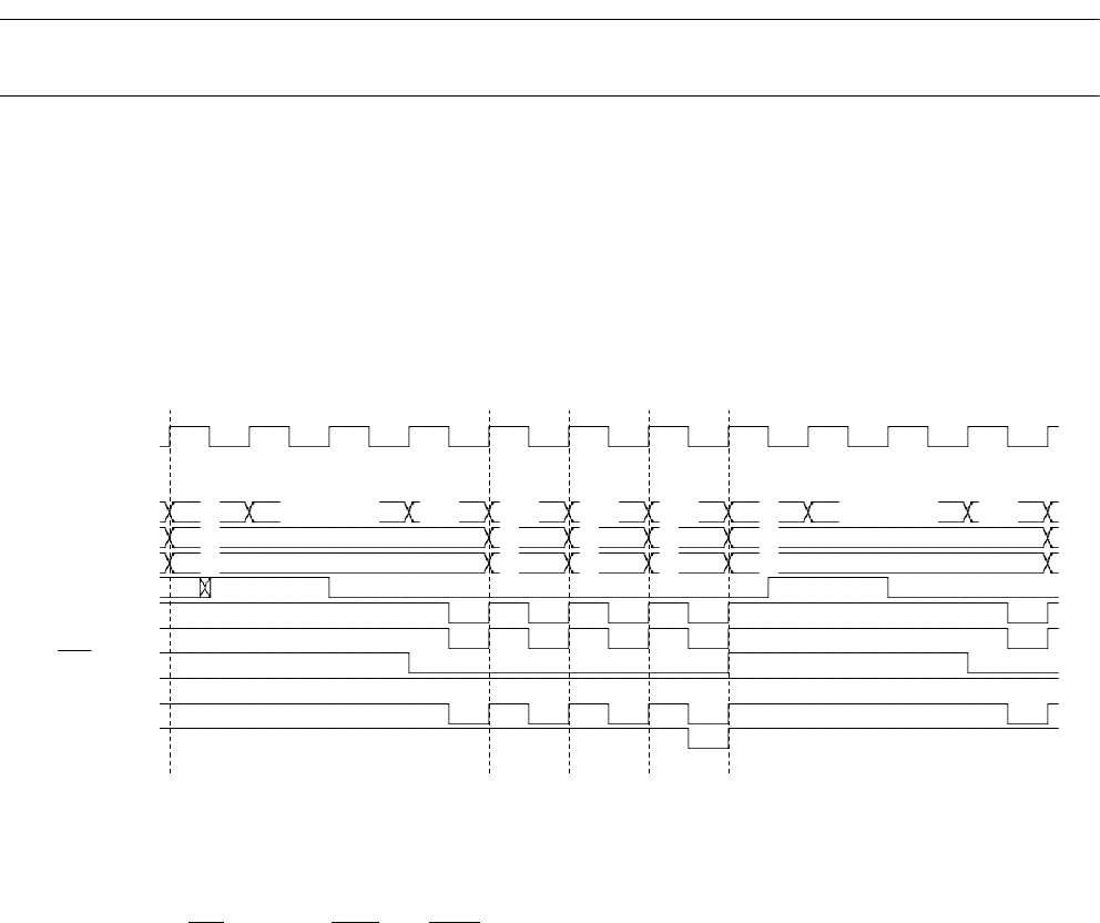
This section provides a hyper DRAM interface write timing chart.
■
Hyper DRAM Interface: Write Timing chart
❍
Bus width: 16 bits, access: words
Figure 4.17-33 Example of Hyper DRAM Interface Write Timing Chart
[Explanation of operation]
• Column addresses and write data are output in Q4HW cycles.
• CAS is asserted at the falling edge of Q4HW and negated at the falling edge of Q4HW.
•WE
(including WEL and WEH) is asserted at the rising edge of the Q4HW cycle and negated
when Q4HW ends.
Q1 Q2 Q3 Q4HW Q4HW Q4HW Q4HW Q1 Q2 Q3 Q4HW
CLK
2CAS/1WE
A24-00
X row.adr. col. col. col. col. X row.adr. col.
D31-24 W W W W W
D23-16 W W W W W
RAS
CASL
CASH
WE
RDX
(DACK0)
(EOP0)
2)


