


183
4.17 Bus Timing
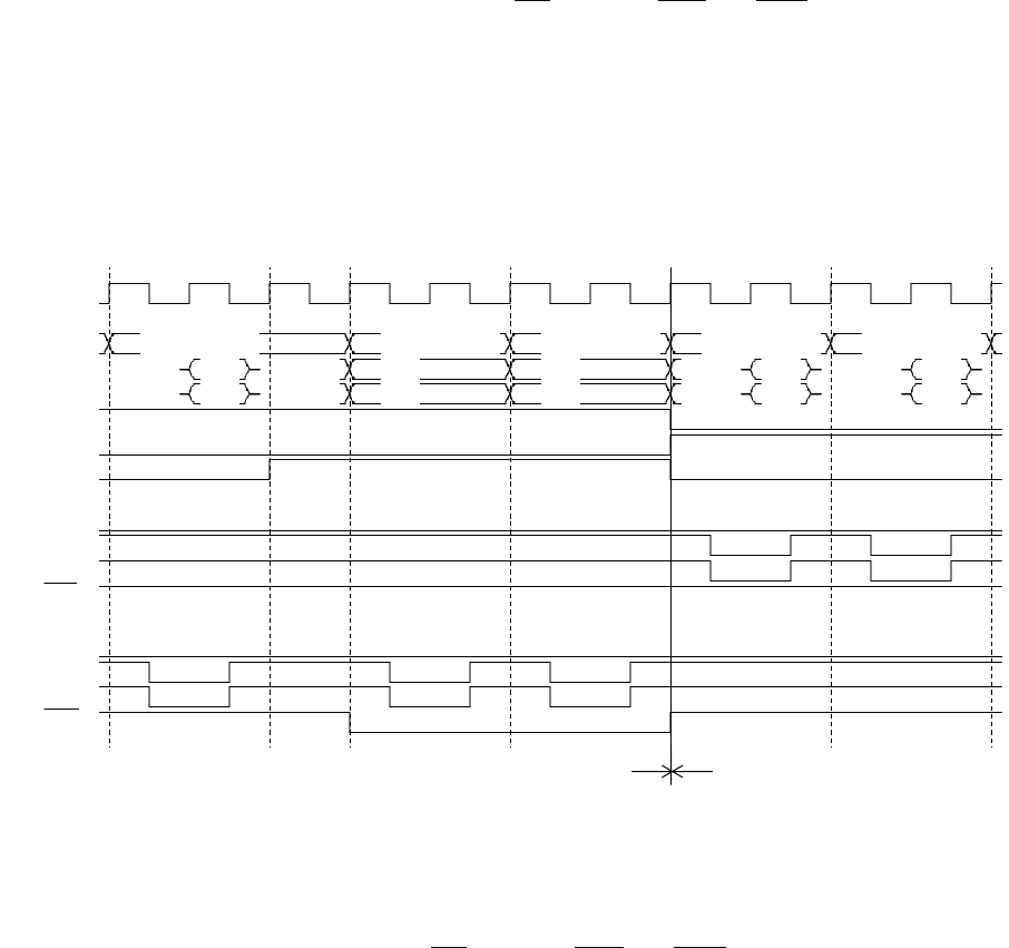
[Explanation of operation]
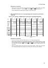
• Write control is performed with only the CAS control signals (including CASL and CASH)
while RAS is lowered to "L", and then WE
(including WEL and WEH) is lowered to "L".
• Column addresses and output data are output in Q4 and Q5 cycles.
❍
CS area (CS4/CS5) switch-over in high-speed page mode, read and write combination,
2CAS/1WE
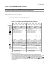
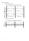
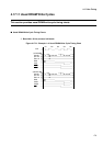
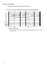
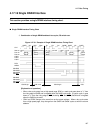
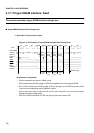
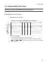
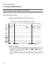
Figure 4.17-27 Example 3 of DRAM Interface Timing Chart in High-Speed Page Mode
[Explanation of operation]
• Even if the CS area is switched, RAS remains at "L" in high-speed page mode.
• When a bus cycle starts from a high-speed page, RDX in a read cycle goes down to "L" from
the rising edge of Q4 and is negated when the Q5 cycle ends. In a write cycle, it goes down
to "L" from the rising edge of WE
(including WEL and WEH) Q4 and is negated when the Q5
cycle ends.
• CS4X and CS5X change at the same time as the output address. When a bus cycle starts
from a high-speed page, they change from the Q4 cycle as with the column address.
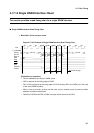
Q4
CLK
A24-00 CS5X col.adr CS5X col.adr CS5X col.adr CS4X col.adr CS4X col.adr
D31-24 Write
D23-16 Read Write
CS4X
CS5X
RDX
CS4:RAS
CS4:CASL
CS4:CASH
CS4:WE
CS5:RAS
CS5:CASL
CS5:CASH
CS5:WE
CS5 area
Q5 Q4 Q5 Q4 Q5 Q4 Q5 Q4 Q5
CS4 area
Idle
Read
Write
Write Read
Read
Read
Read