


136
CHAPTER 4 BUS INTERFACE
4.14 DRAM Signal Control Register (DSCR)
The DRAM signal control register (DSCR) controls the output of each DRAM control
signal. When the output is inhibited, this register can be used as an I/O port.
■
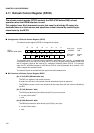
Configuration of DRAM Signal Control Register (DSCR)
The DRAM signal control register (DSCR) is configured as follows:
■
Bit Functions of DRAM Signal Control Register (DSCR)
[bit 7] DW1E
The DW1E bit controls the DW1X output. When this bit is reset, the output is inhibited.
0: Inhibits output (initial value).
1: Permits output.
[bit 6] DW0E
The DW0E bit controls the DW0X output. When this bit is reset, the output is inhibited.
0: Inhibits output (initial value).
1: Permits output.
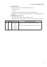
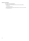
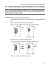
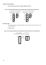
[bit 5] C1HE
The C1HE bit controls the CS1H output. When this bit is reset, the output is inhibited.
In this device type, because the CS1H pin also serves as the DMAC DACK2 output, it is
controlled together with the AKSE2 and AKDE2 bits of the DMAC control register (DATCR)
as shown below.
[bit 4] C1LE
The C1LE bit controls the CS1L output. When this bit is reset, the output is inhibited.
0: Inhibits output (initial value).
1: Permits output.
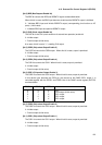
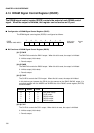
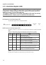
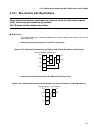
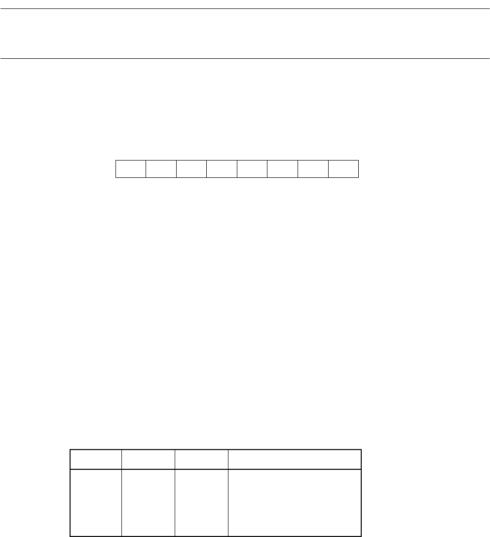
76543210
DSCR
Address: 0000 0625
H
DW1E DW0E C1HE C1LE C0HE C0LE RS1E RS0E 00000000 W
Access
Initial value
AKSE2 AKDE2 C1HE
0
0
0
1
1
0
0
1
0
1
0
1
X
X
X
Port (initial value)
C1HE output
DACK2 output
DACK2 output
DACK2 output