155
4.16 Relationship between Data Bus Widths and Control Signals
4.16.4 DRAM Relationships
This section explains the DRAM relationships.
■
DRAM Control Pins
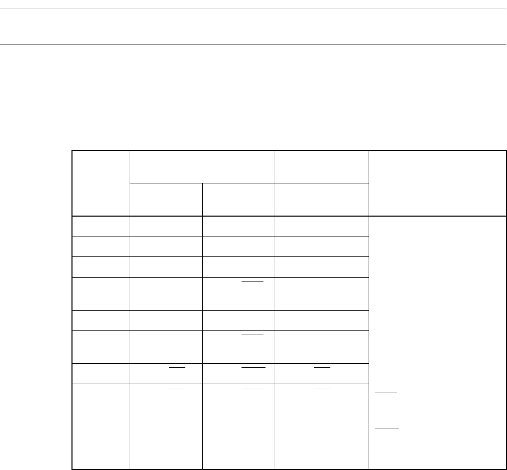
Table 4.16-2 lists the relationship between the pin functions and bus widths used in the DRAM
interface.
Table 4.16-2 Functions and Bus Widths of DRAM Control Pins
Pin name Data bus in 16-bit mode Data bus in 8-bit
mode
Remarks
2CAS/1WE
mode
1CAS/2WE
mode
RAS0 Area 4 RAS Area 4 RAS Area 4 RAS • Correspondence
between "L" and "H"
and lower 1 bit (A0) of
address for data bus in
16-bit mode
• "L":"0"
•"H":"1"
CASL: CAS corresponding
to area containing
"0" in A0
CASH: CAS
corresponding
to area containing
"1" in A0
WEL
: WE corresponding
to area containing
"0" in A0
WEH
: WE corresponding
to area containing
"1" in A0
RAS1 Area 5 RAS Area 5 RAS Area 5 RAS
CS0L Area 4 CASL Area 4 CAS Area 4 CAS
CS0H Area 4
CASH
Area 4 WEL
Area 4 CAS
CS1L Area 5 CASL Area 5 CAS Area 5 CAS
CS1H Area 5
CASH
Area 5 WEL
Area 5 CAS
DW0X Area 4 WE
Area 4 WEH Area 4 WE
DW1X Area 5 WE Area 5 WEH Area 5 WE


