


187
4.17 Bus Timing
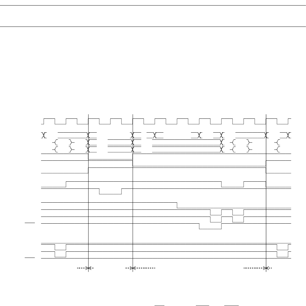
4.17.16 Single DRAM Interface
This section provides a single DRAM interface timing chart.
■
Single DRAM Interface Timing Chart
❍
Combination of single DRAM and basic bus cycle, CS switch-over
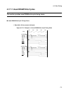
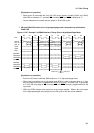
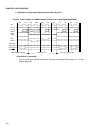
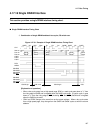
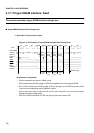
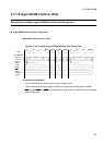
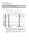
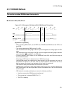
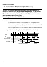
Figure 4.17-31 Example of Single DRAM Interface Timing Chart
[Explanation of operation]
• When a bus cycle starts from a high-speed page, RDX in a read cycle goes down to "L" from
the rising edge of Q4SR and is negated when the Q4SR cycle ends. In a write cycle, it goes
down to "L" from the rising edge of WE
(including WEL and WEH) Q4SW and is negated
when the Q4SW cycle ends.
• CS4X and CS5X change at the same time as the output address. When a bus cycle starts
from a high-speed page, they change from the Q4SR and Q4SW cycles as with the column
address.
Q4SR BA1 BA2 Q1 Q2 Q3 Q4SW Q4SR Q4SR
CLK
A24-00 col. CS2X basic bus X row.adr. col. col. col.
D31-24
D23-16
CS2X
CS4X
CS5X
RDX
WR0X
CS4:RAS
CS4:CASL
CS4:CASH
CS4:WE
CS5:RAS
CS5:CASL
CS5:CASH
CS5:WE
CS5 Single
CS2
usual
CS4 Single CS5
Write
Read
Write
Read
Write
Write
Read
Read
Read
Read
Idle
Idle