


156
CHAPTER 4 BUS INTERFACE
■
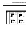
Row and Column Addresses
The page size select bits (PGS3 to PGS0) of DRAM control registers 4 and 5 (DMCR4 and
DMCR5) determines whether to create DRAM interface addresses. When the high-speed page
mode is used, PGS3 to PGS0 and the data bus width determine whether access is within a
page.
When connecting a DRAM, shift the address to be output by this LSI such that it matches the
bus width to be used.
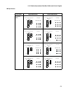
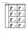
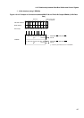
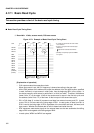
The following is an example of a DRAM connection using an x 8-bit, 256-page size for 8-bit and
16-bit data buses. When the 16-bit data bus is used, one bit of the LSB area of each output
address is left unconnected.
❍
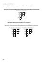
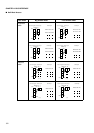
8-bit data bus (using 1 DRAM)
Figure 4.16-18 Example of Connection between MB91F109 and One 8-bit Output DRAM (8-Bit Data Bus)
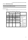
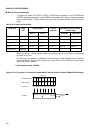
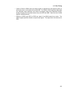
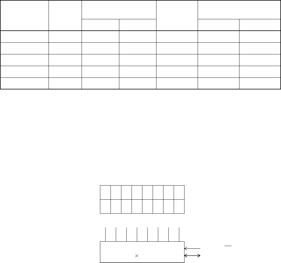
Table 4.16-3 Page Size Select Bits
PGS3 to 0 Page
size
Row address Column
address
Determine whether access
is within page
A31-16 A15-00 8-bit bus 16-bit bus
0000 256 A31-16 A23-08 A31-00 A31-08 A31-09
0001 512 A31-16 A24-09 A31-00 A31-09 A31-10
0010 1024 A31-16 A25-10 A31-00 A31-10 A31-11
0011 4096 A31-16 A27-12 A31-00 A31-12 A31-13
0100 to 1111 reserved - - - - -
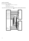
This LSI
COLUMN Address A07 A06 A05 A04 A03 A02 A01 A00
ROW Address A15 A14 A13 A12 A11 A10 A09 A08
External pin A07 A06 A05 A04 A03 A02 A01 A00
A07 A06 A05 A04 A03 A02 A01 A00 RAS,CAS,WE
1 DRAM
D07-00 D31-24
8