


271
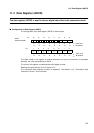
11.2 Control Status Register (ADCS)
<Note>
Set the bit to "0" for clearing it while A/D conversion is stopped.
The bit is initialized to "0" when the register is reset.
A Read Modify Write instruction reads "1" from this bit.
[bit 13] INTE (INTerrupt Enable)
This bit specifies whether to enable issuing interrupt request at the end of conversion.
0: Disable interrupts.
1: Enable interrupts.
Set this bit to "1" for starting DMA transfer by issuing an interrupt. The bit is initialized to "0"
when the register is reset.
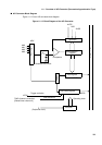
[bit 12] PAUS (A/D converter PAUSe)
This bit is set when A/D conversion stops.
There is only one register that can contain the A/D conversion result. When A/D conversion
is performed continuously, previously stored data is lost unless the conversion result is
transferred by DMA.
This bit is provided to prevent storing the following converted data items until the current
data in the data register is transferred by DMA. A/D conversion is stopped during this
period.
A/D conversion resumes after DMA transfer is finished.
This bit is effective only when DMA is used.
See Section 11.5, "Conversion Data Protection Function," for more information.
The bit is cleared when the register is reset.
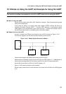
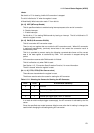
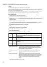
[bit 11, 10] STS1, STS0 (STart Source select)
These bits are cleared when the register is reset.
The bits are used to select the cause for starting the A/D converter.
In a mode for which multiple trigger causes apply, the A/D converter is activated by the first
cause.
Since the specified start mode becomes effective soon after the bit setting is changed, be
careful when changing the bit setting during A/D conversion.
Table 11.2-1 Selecting the Causes for Starting the A/D Converter
STS1 STS0 A/D converter started by
0 0 Software
0 1 External pin trigger signal or software
1 0 Timer or software
1 1 External pin trigger signal, timer, or software