


132
CHAPTER 4 BUS INTERFACE
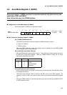
4.12 External Pin Control Register 0 (EPCR0)
External pin control register 0 (EPCR0) controls the output of each signal.
When output is permitted, this register outputs a desired timing signal in each bus
mode. When the input is valid, it receives an input signal from the outside.
When output is inhibited or the input is invalid, the register can be used as an I/O port.
■
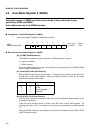
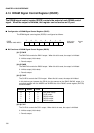
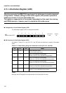
Configuration of External Pin Control Register 0 (EPCR0)
External pin control register 0 (EPCR0) is configured as follows:
■
Bit Functions of External Pin Control Register 0 (EPCR0)
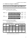
[bit 11] WRE (WRite pulse output Enable bit]
The WRE bit specifies whether to output the WR0X to WR1X write pulses.
When this bit is reset, output is permitted.
0: Inhibits output.
1: Permits output (initial value).
This device type supports no I/O port control for the WR0X to WR1X pins by the WRE bit.
Always set this bit to "1".
Even if the WRE bit is set to "1", the write pulse pin can be used as an I/O port according to
the bus width set by the AMD. (For example, the WR1X pulse is not output in 8-bit mode,
and the corresponding pin can be used as an I/O port.)
[bit 10] RDXE (ReaDX pulse output Enable bit)
The RDXE bit specifies whether to output RDX read pulses.
When this bit is reset, output is permitted.
0: Inhibits output (setting not possible).
1: Permits output (initial value).
When the external bus mode is used, the RDXE bit performs no I/O port control for the RDX
pin. Always set this bit to "1".
[bit 9] RDYE (ReaDY input Enable bit)
The RDYE bit controls the RDY input as described below.
When this bit is reset, the input becomes invalid.
0: Invalidates RDY input (initial value).
1: Validates RDY input.
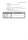
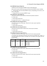
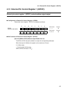
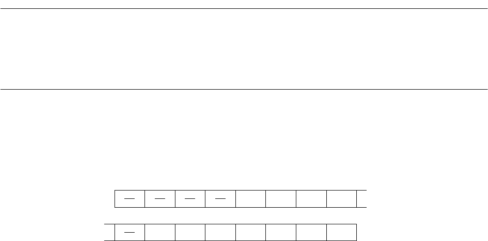
15 14 13 12 11 10 9 8
EPCR0
Address: 0000 0628
H
WRE RDXE RDYE BRE ----1100 W
76543210
CKE COE5 COE4 COE3 COE2 COE1 COE0 -1111111 W
Initial value
Initial value
Access
Access