


17
1.5 Pin Functions
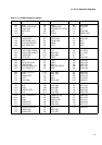
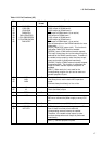
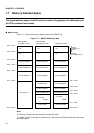
Table 1.5-3 Pin Functions (3/5)
NO. Pin name I/O circuit
format
Function
55
56
57
58
59
60
61
62
RAS0/PB0
CS0L/PB1
CS0H/PB2
DW0X/PB3
RAS1/PB4/EOP2
CS1L/PB5/DREQ2
CS1H/PB6/DACK2
DW1X/PB7
F RAS output of DRAM bank 0
CASL output of DRAM bank 0
CASH output of DRAM bank 0
WE
output of DRAM bank 0 (Low active)
RAS output of DRAM bank 1
CASL output of DRAM bank 1
CASH output of DRAM bank 1
WE
output of DRAM bank 1 (Low active)
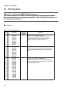
See the description of the DRAM interface for more
information.
[EOP2] DMAC EOP output (ch2). This function is
valid when DMAC EOP output is enabled.
[DREQ2] Input of DMA external transfer request.
This input is used from time to time when this pin is
selected for the DMAC transfer cause. Therefore, it
is needed to stop output by other functions except
when such output is performed intentionally.
[DACK2] Output of DMAC external transfer request
acceptance (ch2). This function is valid when the
output of DMAC transfer request acceptance is
enabled.
[PB0-7] When each pin is not used for the
corresponding purpose, the pin can be used as a
general-purpose I/O port.
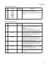
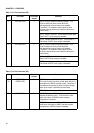
63
64
65
MD0
MD1
MD2
C Mode pins 0 to 2.
Use these pins to set the basic MCU operation
mode.
Connect these pins directly to Vcc or Vss.
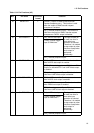
66
67
X0
X1
A Clock (oscillator) input
Clock (oscillator) output
68 RSTX B External reset input
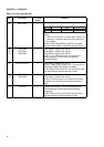
69 VCC - Digital circuit power supply.
Be sure to connect the power supply to every VCC
pin.
70 NMIX D Nonmaskable interrupt (NMI) input (Low active)
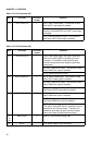
71
72
INT0/PE0
INT1/PE1
F [INT0, 1] Input of external interrupt request. This
input is used from time to time while the
corresponding external interrupt is enabled.
Therefore, it is needed to stop output by other
functions except when such output is performed
intentionally.
[PE0, 1] General-purpose I/O ports