


159
4.17 Bus Timing
4.17 Bus Timing
This section provides bus access timing charts used in each mode and explains bus
access operation for the following items:
• Usual bus access
• Wait cycle
• DRAM interfaceDRAM interface
• DRAM refresh
• External bus request
■
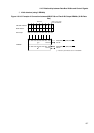
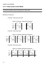
Usual Bus Access
The usual bus interface handles read cycles and write cycles in the same way, as 2-clock
cycles. This manual represents the respective types of cycles as "BA1" and "BA2."
• Basic read cycle
• Basic write cycle
• Read cycle in each mode
• Write cycle in each mode
• Read and write combination cycle
■
Wait Cycles
The wait cycles include automatic wait cycles specified by the WTC bit of the AMD register and
external wait cycles using the RDY pin.
The wait cycles take over the previous cycle and repeat the BA1 cycle until the wait request is
canceled.
• Automatic wait cycle
• External wait cycle
■
DRAM Interface
Chip select areas 4 and 5 can be used as DRAM spaces.
Set the DRME bit of AMD4 or AMD5 to control the operation by DMCR4 and DMCR5.
The DRAM interface has the following three modes, depending on the CAS output, which are
set by the DSAS and HYPR bits of DMCR4 and DMCR5:
• Double CAS access (DSAS: 0, HYPR: 0): usual DRAM interface in this manual
• Single CAS access (DSAS: 1, HYPR: 0): single DRAM interface in this manual
• DRAM with hyper page mode (DSAS: 1, HYPR: 1): hyper DRAM interface in this manual
Set the C/W bit of DMCR4 and DMCR5 to select the 1CAS/2WE DRAM or 2CAS/1WE DRAM.
The page size specified by the PGS3 to PGS0 bits of the DMCR as well as the bus width
specified by the BW1 and BW0 bits of AMD4 or AMD5 determine row and column addresses.