


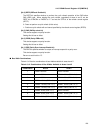

133
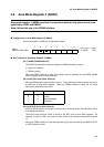
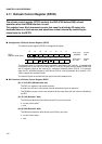
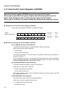
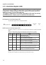
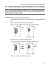
4.12 External Pin Control Register 0 (EPCR0)
[bit 8] BRE (Bus Request Enable bit)
The BRE bit controls the BRQ and BGRNTX signals as described below.
When this bit is reset, the BRQ input becomes invalid and the BGRNTX output is inhibited.
0: Validates BRQ input and inhibits BGRNTX output (corresponding pins function as I/O
ports). (initial value)
1: Validates BRQ input and permits BGRNTX output.
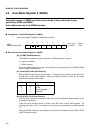
[bit 6] CKE (Clock output Enable bit)
The CKE bit is the CLK (clock waveform of external bus operation) enable bit.
0: Inhibits output.
1: Permits output (initial value).
At a reset, this bit is set to "1", enabling CLK output.
[bit 5] COE5 (Chip select Output Enable 5)
The COE5 bit controls the CS5X output. When this bit is reset, output is permitted.
0: Inhibits output.
1: Permits output (initial value).
[bit 4] COE4 (Chip select Output Enable 4)
The C0E4 bit controls the CS4X. When this bit is reset, output is permitted.
0: Inhibits output.
1: Permits output (initial value).
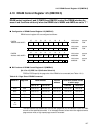
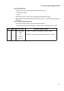
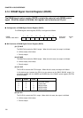
[bit 3] COE 3 (Chip select Output Enable 3)
The C0E3 bit controls the CS3X output. When this bit is reset, output is permitted.
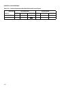
In this device type, because the CS3X pin also serves as the DMAC E0P1 output, it is
controlled together with the EPSE1 and EPDE1 bits of the DMAC control register (DATCR)
as shown below.
[bit 2] COE2 (Chip select Output Enable 2)
The C0E2 bit controls the CS2X output. When this bit is reset, output is permitted.
0: Inhibits output.
1: Permits output (initial value).
[bit 1] COE1 (Chip select Output Enable 1)
The C0E1 bit controls the CS1X output. When this bit is reset, output is permitted.
0: Inhibits output.
1: Permits output (initial value).
EPSE1 EPDE1 COE3
0
0
0
1
1
0
0
1
0
1
0
1
X
X
X
Port
CS3X output (initial value)
E0P1 output
E0P1 output
E0P1 output