27
1.8 Handling of Devices
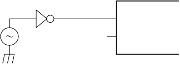
Figure 1.8-2 Example of Using an External Clock (Possible at 12.5 MHz or Lower)
❍
Connection of power pins (Vcc and Vss)
When two or more Vcc or Vss pins are used, the device is designed so that the pins, which
should be at the same potential, are connected to one another inside the device to prevent a
malfunction such as a latchup. However, to minimize unnecessary radiation, prevent strobe
signal malfunction that might be caused by an increase of the ground level, and observe the
total output current standard, be sure to connect all power pins to the power supply and ground
outside.
In addition, consider measures so that impedance is minimized for connection from the power
supply to Vcc and Vss of the device.
It is recommended to insert a ceramic capacitor of about 0.1
µ
F as a bypass capacitor, near the
device, between Vcc and Vss.
❍
Crystal oscillation circuit
Noise generated near the X0 or X1 pin causes the device to malfunction. Design the PC board
so that the X0 and X1 pins, crystal oscillator (or ceramic oscillator), and bypass capacitor to the
ground are located as near to one another as possible. Also, prevent the wiring of these
components from crossing the wiring of other components wherever possible.
Such PC board artwork that places the ground around the X0 and X1 pins is strongly
recommended for stable operation.
❍
Treatment of NC pin
Be sure to keep the NC pin open.
❍
Mode pins (MD0 to MD2)
Connect the mode pins directly to Vcc or Vss.
To prevent malfunction by noise, minimize the pattern length between each mode pin and Vcc
or Vss on the PC board and also minimize impedance for pattern connection.
❍
At power-on
When power is turned on, be sure to begin by putting the RSTX pin in the L level and secure the
time for at least five cycles of the internal operating clock after the power supply reaches the
Vcc level. Put the RSTX pin in the H level only after that.
❍
Pin conditions at power-on
The pin conditions at power-on are unstable. When power is turned on, oscillation begins and
the circuits are initialized.
❍
Input of source oscillation at power-on
When power is turned on, be sure to input clock signals until the oscillation stabilization wait flag
is reset.
X0
OPEN X1
MB91F109


