


8 ELECTRICAL CHARACTERISTICS
A-100 EPSON S1C33L03 PRODUCT PART
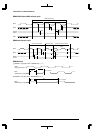
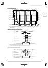
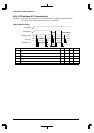
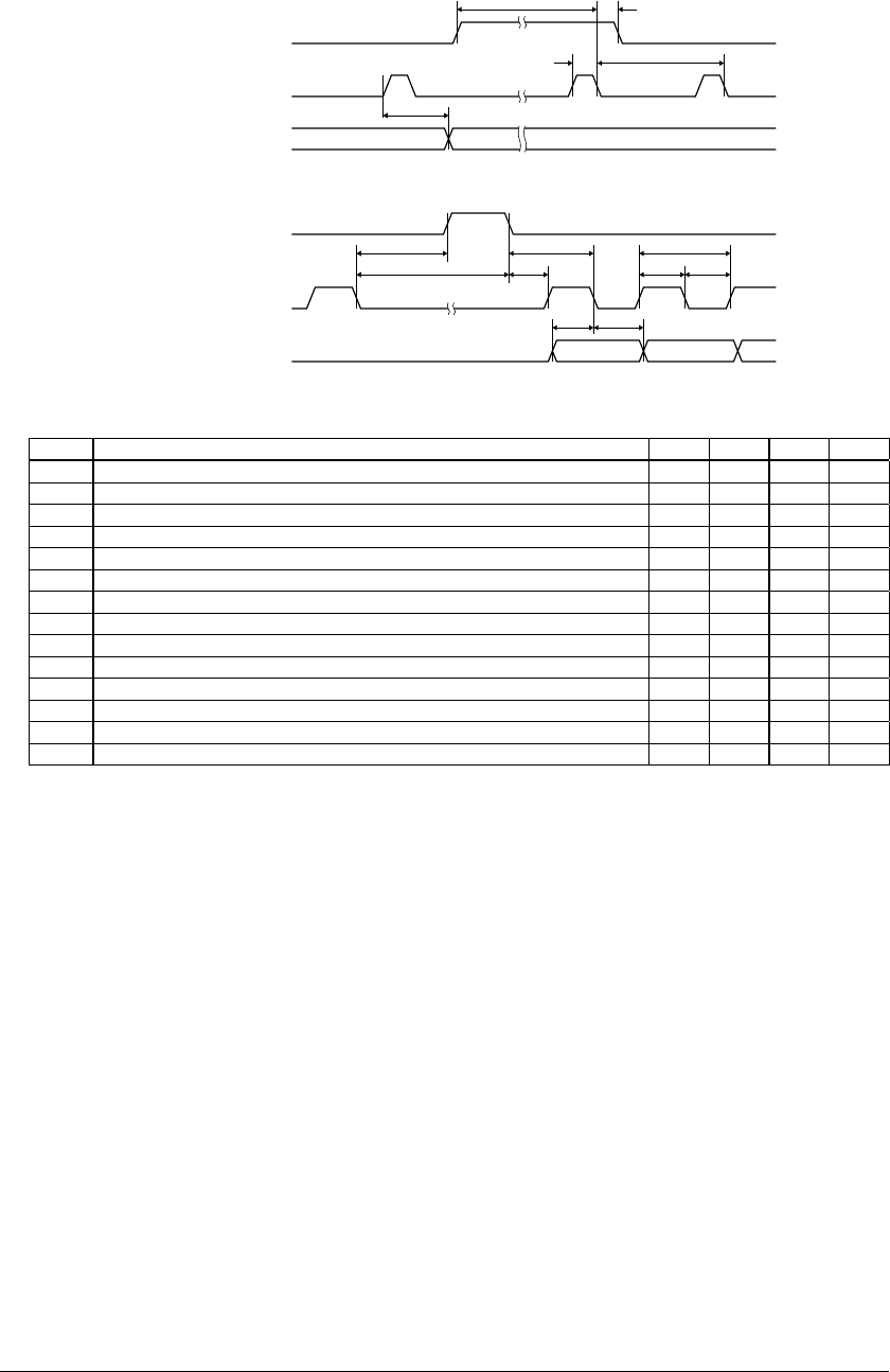
Frame Pulse
Line Pulse
DRDY (MOD)
Sync Timing
21
t2t1
t5
t6 t8 t9
t7 t14 t11 t10
t12 t13
t4 t3
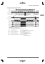
Line Pulse
Shift Pulse
FPDAT[7:0]
Data Timing
Note:For this timing diagram FPSMASK (D2/0x39FFE1) is set to "1".
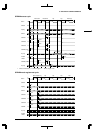
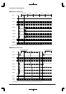
8-bit Single Monochrome Panel AC Timing
Symbol Parameter Min. Typ. Max. Unit
t1 Frame Pulse setup to Line Pulse falling edge note 2 (note 1)
t2 Frame Pulse hold from Line Pulse falling edge 9 Ts
t3 Line Pulse period note 3
t4 Line Pulse width 9 Ts
t5 MOD delay from Line Pulse rising edge 1 Ts
t6 Shift Pulse falling edge to Line Pulse rising edge note 4
t7 Shift Pulse falling edge to Line Pulse falling edge note 5
t8 Line Pulse falling edge to Shift Pulse falling edge t14+4 Ts
t9 Shift Pulse period 8 Ts
t10 Shift Pulse width low 4 Ts
t11 Shift Pulse width high 4 Ts
t12 FPDAT[7:0] setup to Shift Pulse falling edge 4 Ts
t13 FPDAT[7:0] hold from Shift Pulse falling edge 4 Ts
t14 Line Pulse falling edge to Shift Pulse rising edge 23 Ts
note) 1.Ts = pixel clock period
2.t
1min = t3min - 9 (Ts)
3.t
3min = (LDHSIZE[5:0] + 1) × 16 + (HNDP[4:0] + 4) × 8 (Ts)
4.t
6min = HNDP[4:0] × 8 + 4 (Ts)
5.t
7min = HNDP[4:0] × 8 + 13 (Ts)