


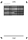

8 ELECTRICAL CHARACTERISTICS
A-78 EPSON S1C33L03 PRODUCT PART
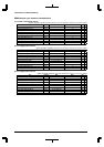
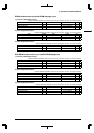
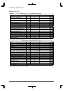
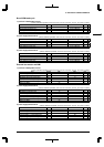
8.6 AC Characteristics
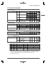
8.6.1 Symbol Description
tCYC: Bus-clock cycle time
• In x1 mode,
tCYC = 50 ns (20 MHz) when the CPU is operated with a 20-MHz clock
tCYC = 30 ns (33 MHz) when the CPU is operated with a 33-MHz clock
• In x2 mode,
tCYC = 50 ns (20 MHz) when the CPU is operated with a 40-MHz clock
tCYC = 40 ns (25 MHz) when the CPU is operated with a 50-MHz clock
tCYC = 33 ns (30 MHz) when the CPU is operated with a 60-MHz clock
WC: Number of wait cycles
Up to 7 cycles can be set for the number of cycles using the BCU control register. Furthermore, it can be
extended to a desired number of cycles by setting the #WAIT pin from outside of the IC.
The minimum number of read cycles with no wait (0) inserted is 1 cycle.
The minimum number of write cycles with no wait cycle (0) inserted is 2 cycles. It does not change even if
1-wait cycle is set. The write cycle is actually extended when 2 or more wait cycles are set.
When inserting wait cycles by controlling the #WAIT pin from outside of the IC, pay attention to the
timing of the #WAIT signal sampling. Read cycles are terminated at the cycle in which the #WAIT signal
is negated. Write cycles are terminated at the following cycle after the #WAIT signal is negated.
C1, C2, C3, Cn: Cycle number
C1 indicates the first cycle when the BCU transfers data from/to an external memory or another device.
Similarly, C2 and Cn indicate the second cycle and nth cycle, respectively.
Cw: Wait cycle
Indicates that the cycle is wait cycle inserted.
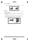
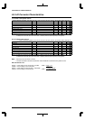
8.6.2 AC Characteristics Measurement Condition
Signal detection level: Input signal High level VIH = VDDE - 0.4 V
Low level V
IL = 0.4 V
Output signal High level V
OH = 1/2 VDDE
Low level VOL = 1/2 VDDE
The following applies when OSC3 is external clock input:
Input signal High level V
IH = 1/2 VDD
Low level VIL = 1/2 VDD
Input signal waveform: Rise time (10% → 90% VDD)5 ns
Fall time (90% → 10% V
DD)5 ns
Output load capacitance: C
L = 50 pF