


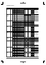
4 PERIPHERAL CIRCUITS
A-38 EPSON S1C33L03 PRODUCT PART
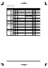
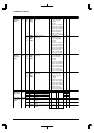
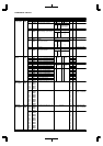
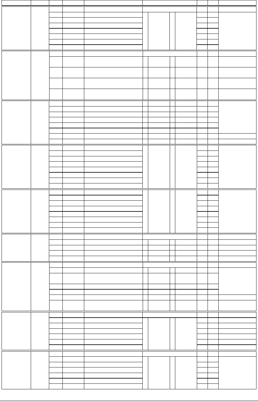
NameAddressRegister name Bit Function Setting Init. R/W Remarks
–
IOC16
IOC15
IOC14
IOC13
IOC12
IOC11
IOC10
D7
D6
D5
D4
D3
D2
D1
D0
reserved
P16 I/O control
P15 I/O control
P14 I/O control
P13 I/O control
P12 I/O control
P11 I/O control
P10 I/O control
–
0
0
0
0
0
0
0
–
R/W
R/W
R/W
R/W
R/W
R/W
R/W
0 when being read.
This register
indicates the values
of the I/O control
signals of the ports
when it is read. (See
detailed explanation.)
00402D6
(B)
1 Output 0 Input
–P1 I/O control
register
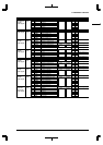
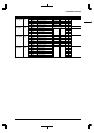
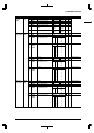
–
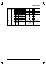
SSRDY3
SSCLK3
SSOUT3
SSIN3
D7–4
D3
D2
D1
D0
reserved
Serial I/F Ch.3 SRDY selection
Serial I/F Ch.3 SCLK selection
Serial I/F Ch.3 SOUT selection
Serial I/F Ch.3 SIN selection
– –
0
0
0
0
–
R/W
R/W
R/W
R/W
00402D7Port SIO
function
extension
register
1 #SRDY3 0
P32/
#DMAACK0
1 #SCLK3 0
P15/EXCL4/
#DMAEND0
1 SOUT3 0
P16/EXCL5/
#DMAEND1
1 SIN3 0
P33/
#DMAACK1
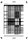
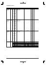
CFP27
CFP26
CFP25
CFP24
CFP23
CFP22
CFP21
CFP20
D7
D6
D5
D4
D3
D2
D1
D0
P27 function selection
P26 function selection
P25 function selection
P24 function selection
P23 function selection
P22 function selection
P21 function selection
P20 function selection
0
0
0
0
0
0
0
0
R/W
R/W
R/W
R/W
R/W
R/W
R/W
R/W
Ext. func.(0x402DF)
00402D8
(B)
1 TM5 0 P27
1 TM4 0 P26
1 TM3 0 P25
1 TM2 0 P24
1 TM1 0 P23
1 TM0 0 P22
1 #DWE 0 P21
1 #DRD 0 P20
P2 function
select register
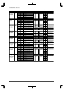
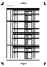
P27D
P26D
P25D
P24D
P23D
P22D
P21D
P20D
D7
D6
D5
D4
D3
D2
D1
D0
P27 I/O port data
P26 I/O port data
P25 I/O port data
P24 I/O port data
P23 I/O port data
P22 I/O port data
P21 I/O port data
P20 I/O port data
0
0
0
0
0
0
0
0
R/W
R/W
R/W
R/W
R/W
R/W
R/W
R/W
00402D9
(B)
1 High 0 LowP2 I/O port data
register
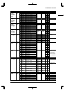
IOC27
IOC26
IOC25
IOC24
IOC23
IOC22
IOC21
IOC20
D7
D6
D5
D4
D3
D2
D1
D0
P27 I/O control
P26 I/O control
P25 I/O control
P24 I/O control
P23 I/O control
P22 I/O control
P21 I/O control
P20 I/O control
0
0
0
0
0
0
0
0
R/W
R/W
R/W
R/W
R/W
R/W
R/W
R/W
This register
indicates the values
of the I/O control
signals of the ports
when it is read. (See
detailed explanation.)
00402DA
(B)
1 Output 0 InputP2 I/O control
register
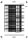
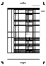
–
SSRDY2
SSCLK2
SSOUT2
SSIN2
D7–4
D3
D2
D1
D0
reserved
Serial I/F Ch.2 SRDY selection
Serial I/F Ch.2 SCLK selection
Serial I/F Ch.2 SOUT selection
Serial I/F Ch.2 SIN selection
–
0
0
0
0
–
R/W
R/W
R/W
R/W
00402DB
1 #SRDY2 0 P24/TM2
1 #SCLK2 0 P25/TM3
1 SOUT2 0 P26/TM4
1 SIN2 0 P27/TM5
Port SIO
function
extension
register
–
–
CFP35
CFP34
CFP33
CFP32
CFP31
CFP30
D7–6
D5
D4
D3
D2
D1
D0
reserved
P35 function selection
P34 function selection
P33 function selection
P32 function selection
P31 function selection
P30 function selection
–
0
0
0
0
0
0
–
R/W
R/W
R/W
R/W
R/W
R/W
0 when being read.
Ext. func.(0x402DF)
00402DC
(B)
–P3 function
select register
1 #BUSACK 0 P35
1 #BUSREQ
#CE6
0 P34
1
#DMAACK0
0 P32
1 #BUSGET 0 P31
1 #WAIT
#CE4/#CE5
0 P30
1
#DMAACK1
0 P33
–
P35D
P34D
P33D
P32D
P31D
P30D
D7–6
D5
D4
D3
D2
D1
D0
reserved
P35 I/O port data
P34 I/O port data
P33 I/O port data
P32 I/O port data
P31 I/O port data
P30 I/O port data
–
0
0
0
0
0
0
–
R/W
R/W
R/W
R/W
R/W
R/W
0 when being read.00402DD
(B)
1 High 0 Low
–
P3 I/O port data
register
–
IOC35
IOC34
IOC33
IOC32
IOC31
IOC30
D7–6
D5
D4
D3
D2
D1
D0
reserved
P35 I/O control
P34 I/O control
P33 I/O control
P32 I/O control
P31 I/O control
P30 I/O control
–
0
0
0
0
0
0
–
R/W
R/W
R/W
R/W
R/W
R/W
0 when being read.
This register
indicates the values
of the I/O control
signals of the ports
when it is read. (See
detailed explanation.)
00402DE
(B)
1 Output 0 Input
–P3 I/O control
register