


III PERIPHERAL BLOCK: INPUT/OUTPUT PORTS
B-III-9-2 EPSON S1C33L03 FUNCTION PART
Input-Port Pins
The input pins concurrently serve as the input pins for peripheral circuits, as shown in Table 9.1. Whether they are
used as input ports or for peripheral circuits can be set bit-for-bit using a function select register. All pins not used
for peripheral circuits can be used as general-purpose input ports that have an interrupt function.
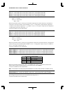
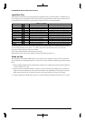
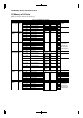
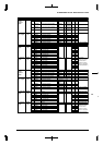
Table 9.1 Input Pins
Pin name I/O Pull-up Function Function select bit
K50/#DMAREQ0 IAvailable Input port / High-speed DMA request 0 CFK50(D0)/K5 function select register(0x402C0)
K51/#DMAREQ1 IAvailable Input port / High-speed DMA request 1 CFK51(D1)/K5 function select register(0x402C0)
K52/#ADTRG IAvailable Input port / AD converter trigger CFK52(D2)/K5 function select register(0x402C0)
K53/#DMAREQ2 IAvailable Input port / High-speed DMA request 2 CFK53(D3)/K5 function select register(0x402C0)
K54/#DMAREQ3 IAvailable Input port / High-speed DMA request 3 CFK54(D4)/K5 function select register(0x402C0)
K60/AD0 I–Input port / AD converter input 0 CFK60(D0)/K6 function select register(0x402C3)
K61/AD1 I–Input port / AD converter input 1 CFK61(D1)/K6 function select register(0x402C3)
K62/AD2 I–Input port / AD converter input 2 CFK62(D2)/K6 function select register(0x402C3)
K63/AD3 I–Input port / AD converter input 3 CFK63(D3)/K6 function select register(0x402C3)
K64/AD4 I–Input port / AD converter input 4 CFK64(D4)/K6 function select register(0x402C3)
K65/AD5 I–Input port / AD converter input 5 CFK65(D5)/K6 function select register(0x402C3)
K66/AD6 I–Input port / AD converter input 6 CFK66(D6)/K6 function select register(0x402C3)
K67/AD7 I–Input port / AD converter input 7 CFK67(D7)/K6 function select register(0x402C3)
At cold start, all pins are set for input ports Kxx (function select register CFKxx = "0"). When these pins are used
for the internal peripheral circuits, write "1" to CFKxx. For details on pin functions in this case, refer to the
description of each peripheral circuit in this manual.
At hot start, the pins retain their state from prior to the reset.
When the ports set for A/D converter input are read, the value obtained is always "0".
Notes on Use
The input buffers of the K50 and K60 to K67 ports use AVDDE (power voltage for A/D converter) as their power
source. Furthermore, the K50 pull-up resistor is connected to AV
DDE. Therefore, the following precautions must be
taken.
1) When using K50 and K60–K67 as general-purpose input ports, the voltage input to the port must be high level
= AV
DDE and low level = VSS.
2) When using V
DDE as high level similar to other ports, VDDE must be the same voltage level as AVDDE. If the
input V
DDE level is lower than the AVDDE level, current flows in the input buffer, or if the input VDDE level is
higher than the AV
DDE level, current flows from the VDDE power supply to the AVDDE power supply.
3) To fix the input level externally when the port is not used, the input pin should be connected to V
SS or AVDDE.