II CORE BLOCK: BCU (Bus Control Unit)
B-II-4-46 EPSON S1C33L03 FUNCTION PART
A18RD:Areas 18–17 read signal (D7) / G/A read signal control register (0x48138)
A16RD:Areas 16–15 read signal (D6) / G/A read signal control register (0x48138)
A14RD:Areas 14–13 read signal (D5) / G/A read signal control register (0x48138)
A12RD:Areas 12–11 read signal (D4) / G/A read signal control register (0x48138)
A8RD:Areas 8–7 read signal (D2) / G/A read signal control register (0x48138)
A6RD:Area 6 read signal (D1) / G/A read signal control register (0x48138)
A5RD:Areas 5–4 read signal (D0) / G/A read signal control register (0x48138)
Enable/disable the exclusive read signal output.
Write "1": Enabled
Write "0": Disabled
Read: Valid
If AxxRD is set to "1", the exclusive read signal is output from #GARD (P31) pin when the corresponding area is
read. If AxxRD is set to "0", the signal output is disabled.
At cold start, these bits are set to "0" (disabled). At hot start, these bits retain their status before being initialized.
BCLKSEL1–BCLKSEL0: BCLK output clock selection (D[1:0]) / BCLK select register (0x4813A)
Select a clock to be output from the BCLK pin. These bits are effective only when SDRENA (D7/0x39FFC1) is
"0".
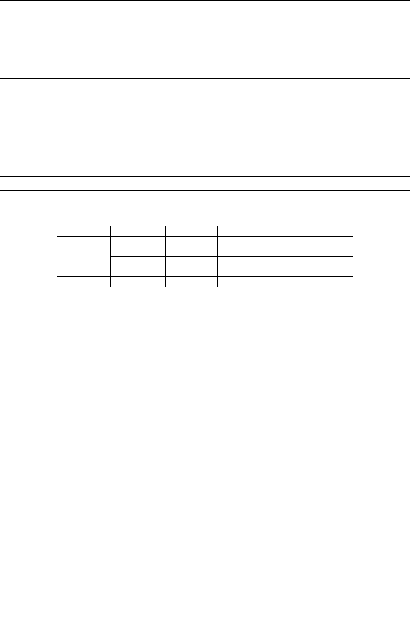
Table 4.32 Selection of BCLK Output Clock
SDRENA BCLKSEL1 BCLKSEL0 Output clock
11PLL_CLK (PLL output clock)
10OSC3_CLK (OSC3 oscillation clock)
01BCU_CLK (BCU operating clock)
0
00CPU_CLK (CPU operating clock)
1––SD_CLK (SDRAM clock)
PLL_CLK: PLL output clock. This clock is stable and kept as output except in the following cases:
1. When the PLL is off by setting the PLLS[1:0] pins.
2. When the OSC3 (high-speed) oscillation is stopped by executing the SLP instruction.
3. When the OSC3 (high-speed) oscillation is stopped using the CLG register.
Note that the PLL_CLK clock is out of phase with the CPU operating clock.
OSC3_CLK: OSC3 (high-speed) oscillation circuit output clock. This clock is stable and kept as output except in
the following cases:
1. When the OSC3 (high-speed) oscillation is stopped by executing the SLP instruction.
2. When the OSC3 (high-speed) oscillation is stopped using the CLG register.
Note that the OSC3_CLK clock is out of phase with the CPU operating clock.
BCU_CLK: Bus clock in the bus controller. This clock varies according to the bus cycle speed. Furthermore, the
clock frequency changes dynamically in x2 speed mode as follows:
1. When the internal RAM/ROM is accessed, x2 clock (e.g., 50 MHz same as the CPU operating
clock) is output.
2. When an external device is accessed via the external bus, x1 clock (e.g., 25 MHz) is output.
This dynamic change (e.g., between 50 MHz and 25 MHz) does not affect the external memory
access timing, such as position relationship between the rising or falling edge of the 25 MHz clock
and the falling edge of the #WR signal. (It is the same as that in the x1 speed mode with 25 MHz
clock.)
CPU_CLK: The CPU operating clock. The clock frequency is as follows:
1. Equals to the PLL output clock frequency when the PLL is on.
2. Equals to the OSC3 (high-speed) oscillation circuit output clock frequency when the PLL is off.
3. However, it equals to the divided frequency when the CLG is set to generate the CPU operating
clock by dividing the source clock.
4. When the CPU stops by the HALT or SLP instruction, this clock is also stopped.
This clock is almost in phase with the bus clock.
At initial reset, BCLKSEL is set to "00" (CPU_CLK).


