


8 ELECTRICAL CHARACTERISTICS
S1C33L03 PRODUCT PART EPSON A-83
A-1
A-8
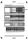
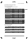
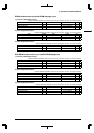
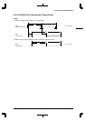
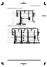
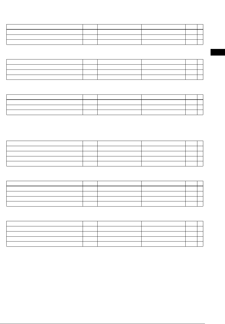
DRAM random access cycle and DRAM fast-page cycle
1) 3.3 V/5.0 V dual power source
(Unless otherwise specified: VDDE=5.0V±0.5V, VDD=2.7V to 3.6V, VSS=0V, Ta=-40°C to +85°C)
Item Symbol Min. Max. Unit ∗
Column address access time tACCF tCYC(1+WC)-25 ns
#RAS access time tRACF tCYC(1.5+WC)-25 ns
#CAS access time tCACF tCYC(0.5+WC)-25 ns
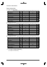
2) 3.3 V single power source
(Unless otherwise specified: VDDE=VDD=2.7V to 3.6V, VSS=0V, Ta=-40°C to +85°C)
Item Symbol Min. Max. Unit ∗
Column address access time tACCF tCYC(1+WC)-25 ns
#RAS access time tRACF tCYC(1.5+WC)-25 ns
#CAS access time tCACF tCYC(0.5+WC)-25 ns
3) 2.0 V single power source
(Unless otherwise specified: VDDE=VDD=2.0V±0.2V, VSS=0V, Ta=-40°C to +85°C)
Item Symbol Min. Max. Unit ∗
Column address access time tACCF tCYC(1+WC)-60 ns
#RAS access time tRACF tCYC(1.5+WC)-60 ns
#CAS access time tCACF tCYC(0.5+WC)-60 ns
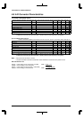
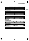
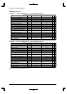
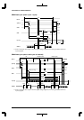
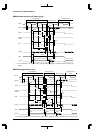
EDO DRAM random access cycle and EDO DRAM page cycle
1) 3.3 V/5.0 V dual power source
(Unless otherwise specified: VDDE=5.0V±0.5V, VDD=2.7V to 3.6V, VSS=0V, Ta=-40°C to +85°C)
Item Symbol Min. Max. Unit ∗
Column address access time tACCE tCYC(1.5+WC)-25 ns
#RAS access time tRACE tCYC(2+WC)-25 ns
#CAS access time tCACE tCYC(1+WC)-15 ns
Read data setup time tRDS2 20 ns
2) 3.3 V single power source
(Unless otherwise specified: VDDE=VDD=2.7V to 3.6V, VSS=0V, Ta=-40°C to +85°C)
Item Symbol Min. Max. Unit ∗
Column address access time tACCE tCYC(1.5+WC)-25 ns
#RAS access time tRACE tCYC(2+WC)-25 ns
#CAS access time tCACE tCYC(1+WC)-20 ns
Read data setup time tRDS2 20 ns
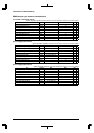
3) 2.0 V single power source
(Unless otherwise specified: VDDE=VDD=2.0V±0.2V, VSS=0V, Ta=-40°C to +85°C)
Item Symbol Min. Max. Unit ∗
Column address access time tACCE tCYC(1.5+WC)-60 ns
#RAS access time tRACE tCYC(2+WC)-60 ns
#CAS access time tCACE tCYC(1+WC)-60 ns
Read data setup time tRDS2 20 ns