


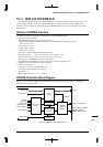

VI SDRAM CONTROLLER BLOCK: SDRAM INTERFACE
S1C33L03 FUNCTION PART EPSON B-VI-2-9
A-1
B-VI
SDRAM
Selecting initialization sequence
The SDRAM command sequence that is run immediately after SDRAM power-up can be selected to suit the
specifications of the SDRAM used. For this setting, use the SDRIS (D4)/SDRAM control register
(0x39FFC1).
SDRIS = "0": 1. Precharge → 2. Refresh → 3. Mode Register Set
SDRIS = "1": 1. Precharge → 2. Mode Register Set → 3. Refresh
If no problems are incurred in either setting, SDRIS = "1" is recommended.
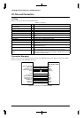
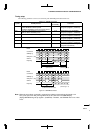
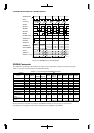
Burst length
The burst length can be selected using the SDRBL[1:0] (D[3:2])/SDRAM mode set-up register (0x39FFC3).
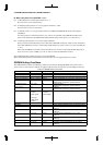
Table 2.9 Setting Burst Length
SDRBL1 SDRBL0 Burst length (word)
00 1
01 2
10 4
11 8 (default)
Notes:•Burst transfers are effective only when reading data from SDRAM. When writing to SDRAM,
data are always written in a single operation, not in bursts, no matter what burst length is
selected.
•The SDRAM controller is designed in such a way that when one cycle of burst read is finished,
it automatically issues the READ command to continue with transfers. Therefore, unless
SDRBL[1:0] = "00", the speed at which SDRAM is accessed does not vary with the burst length
involved.
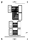
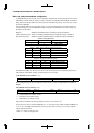
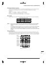
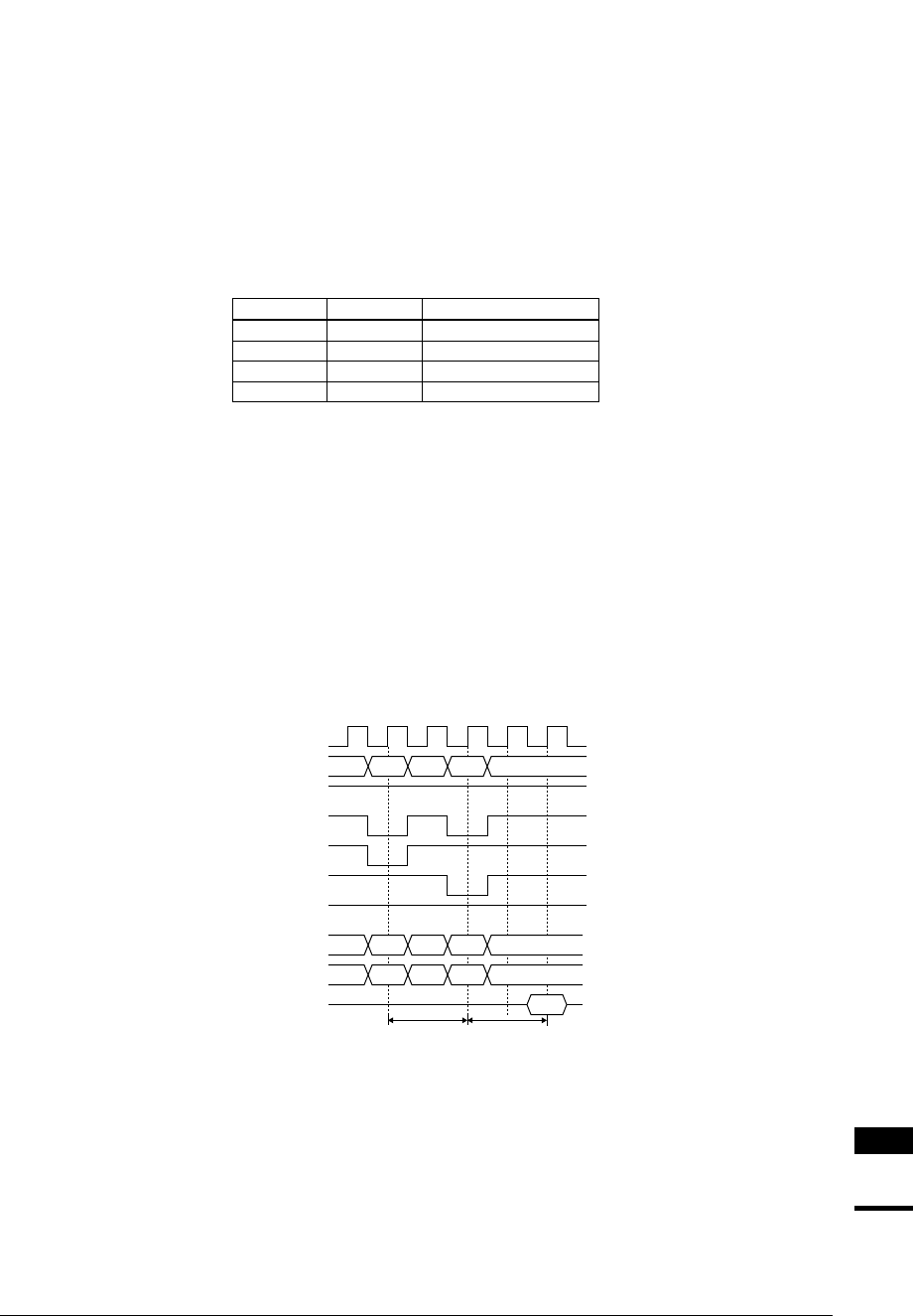
Setting CAS latency
The CAS latency is defined by the number of clock cycles before data is output from SDRAM after issuing
the READ command and this SDRAM controller supports only 2 clocks of CAS latency. Set the SDRCL[1:0]
(D[6:5])/SDRAM mode set-up register (0x39FFC3) to "10" (CAS latency = 2) before accessing the SDRAM.
BCLK
Command
SDCKE
#SDCEx
#SDRAS
#SDCAS
#SDWE
SDBA[1:0]
SDA[12:0]
DQ[15:0]
ACTVNOP NOP NOPREAD
BA BA
ROW COL
DATA
t
RCD
CAS latency = 2
Figure 2.5 CAS Latency