


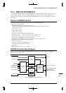

VI SDRAM CONTROLLER BLOCK: SDRAM INTERFACE
B-VI-2-8 EPSON S1C33L03 FUNCTION PART
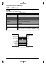
Bank, row, and column address configuration
An SDRAM memory array consists of two or four banks, with each bank divided into pages. For this reason,
SDRAMs have a bank select pin which is not found in asynchronous DRAMs. Inside the Bank, the Column
(Page) address and the Row address are selected by #CAS and #RAS, respectively, in the same way as with
asynchronous DRAMs.
For the SDRAM addresses to be generated correctly, it is necessary that the bank size and the column and
row address ranges be set in the SDRAM controller according to the SDRAMs used. For these settings, use
the registers shown below.
Bank size: SDRBA (D1)/SDRAM address configuration register (0x39FFC2)
Column addressing range: SDRCA[1:0] (D[6:5])/SDRAM address configuration register (0x39FFC2)
Row addressing range: SDRRA[1:0] (D[3:2])/SDRAM address configuration register (0x39FFC2)
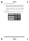
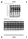
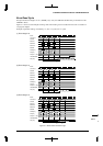
Table 2.6 Setting Bank Size
SDRBA Number of banks Bank address (pin) used
02SDBA0 (default)
14SDBA0–SDBA1
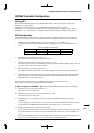
Table 2.7 Setting Column Addressing Range (Page Size)
SDRCA1 SDRCA0 Column size Column address (pin) used
00 256SDA0–SDA7 (default)
01 512 SDA0–SDA8
10 1,024 SDA0–SDA9
11 – –
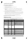
Table 2.8 Setting Row Addressing Range
SDRRA1 SDRRA0 Row size Row address (pin) used
00 2KSDA0–SDA10 (default)
01 4K SDA0–SDA11
10 8K SDA0–SDA12
11 – –
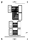
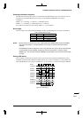
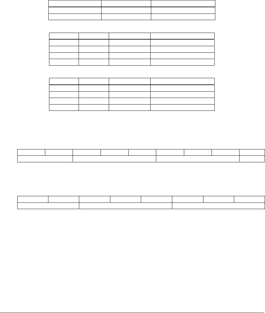
The SDRAM controller uses only the lower 24 bits of the 28-bit address bus. The relationship between the
CPU addresses and the Bank, Column, and Row addresses is shown below.
16-bit SDRAM interface (SDRSZ = "1")
A(m+n+p) A(m+n+1) A(m+n) ··· A(m+1) A(m) ··· A1 A0
Bank address Row address Column address DQM
When reading/writing byte data, the SDRAM controller decodes A0/BSL and WRH/BSH into LDQM and
HDQM.
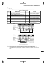
8-bit SDRAM interface (SDRSZ = "0")
A(m+n+p-1) A(m+n) A(m+n-1) ··· A(m) A(m-1) ··· A0
Bank address Row address Column address
m: Column address size (number of bits)
n: Row address size (number of bits)
p: Bank address size (number of bits)
Upper address bits that are not used (depending on memory size) are all set to 0s.
In cases when two areas are selected (SDRAR[1:0] = "11") and only one chip enable is enabled (SDRPC[1:0]
= "01" or "10"), the MSB of the bank address (A(m+n+p) for 16 bits or A(m+n+p-1) for 8 bits) is replaced
with the value shown below.
• Value is "0" when accessing area 7/13
• Value is "1" when accessing area 8/14