


III PERIPHERAL BLOCK: PRESCALER
S1C33L03 FUNCTION PART EPSON B-III-2-7
A-1
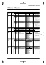
B-III
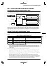
PSC
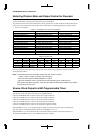
P16TON0:16-bit timer 0 clock control (D3) / 16-bit timer 0 clock control register (0x40147)
P16TON1:16-bit timer 1 clock control (D3) / 16-bit timer 1 clock control register (0x40148)
P16TON2:16-bit timer 2 clock control (D3) / 16-bit timer 2 clock control register (0x40149)
P16TON3:16-bit timer 3 clock control (D3) / 16-bit timer 3 clock control register (0x4014A)
P16TON4:16-bit timer 4 clock control (D3) / 16-bit timer 4 clock control register (0x4014B)
P16TON5:16-bit timer 5 clock control (D3) / 16-bit timer 5 clock control register (0x4014C)
P8TON0:8-bit timer 0 clock control (D3) / 8-bit timer 0/1 clock control register (0x4014D)
P8TON1:8-bit timer 1 clock control (D7) / 8-bit timer 0/1 clock control register (0x4014D)
P8TON2:8-bit timer 2 clock control (D3) / 8-bit timer 2/3 clock control register (0x4014E)
P8TON3:8-bit timer 3 clock control (D7) / 8-bit timer 2/3 clock control register (0x4014E)
P8TON4:8-bit timer 4 clock control (D3) / 8-bit timer 4/5 clock control register (0x40145)
P8TON5:8-bit timer 5 clock control (D7) / 8-bit timer 4/5 clock control register (0x40145)
PSONAD:A/D converter clock control (D3) / A/D clock control register (0x4014F)
Control the clock supply to each peripheral circuit.
Write "1": On
Write "0": Off
Read: Valid
The clock selected using the division ratio setup bits is output to the corresponding peripheral circuit by writing "1"
to these bits.
The clock is not output by writing "0". If the peripheral circuits do not need to be operated, write "0" to these bits.
This helps to reduce current consumption.
At initial reset, all of these bits are set to "0" (Off).
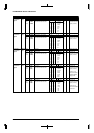
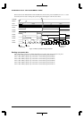
P8TPCK0: 8-bit timer 0 clock selection (D0) / 8-bit timer clock select register (0x40146)
P8TPCK1: 8-bit timer 1 clock selection (D1) / 8-bit timer clock select register (0x40146)
P8TPCK2: 8-bit timer 2 clock selection (D2) / 8-bit timer clock select register (0x40146)
P8TPCK3: 8-bit timer 3 clock selection (D3) / 8-bit timer clock select register (0x40146)
P8TPCK4: 8-bit timer 4 clock selection (D0) / 8-bit timer 4/5 clock select register (0x40140)
P8TPCK5: 8-bit timer 5 clock selection (D1) / 8-bit timer 4/5 clock select register (0x40140)
Select the operating clock for the 8-bit programmable timer.
Write "1": Prescaler input clock (θ/1)
Write "0": Divided clock
Read: Valid
When "1" is written to P8TPCKx, the prescaler input clock (θ/1) is selected for the 8-bit timer x operating clock.
The clock output is controlled by the P8TONx bit even if P8TPCKx is set to "1".
When "0" is written, the divided clock that is selected by P8TSx[2:0] will be output to the 8-bit timer x.
At initial reset, P8TPCKx is set to "0" (divided clock).