VII LCD CONTROLLER BLOCK: LCD CONTROLLER
S1C33L03 FUNCTION PART EPSON B-VII-2-3
A-1
B-VII
LCDC
Block Diagram
#BUSREQ
#BUSACK
#BUSGET
#CE7/13(8/14)
Address[23:0]
Data[15:0]
#CE6
FIFO Display
pipeline
Sequence
controller
DMA
interface
Bus
interface
Control
registers
Look-up
table
Frame rate
modulation
LCD
interface
FPDAT[7:0]
FPFRAME
FPLINE
FPSHIFT
DRDY
LCDPWR
To SDRAM Controller
User logic signals
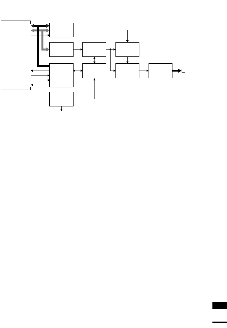
Figure 2.1 Block Diagram of the LCD Controller
Bus interface
The LCD controller is mapped into area 6, along with the SDRAM controller. Area 6 is internally accessed
for read/write to the control registers.
DMA interface
The display data is taken in from the display frame buffer by means of a DMA transfer.
Address generator
This generates the memory addresses for the display data to be taken in by means of a DMA transfer.
FIFO
This is a 16 × 16-bit FIFO used to write data into the display frame buffer and look-up table.
Look-up table
This consists of three 16 × 4-bit palettes (red, green, and blue).
During grayscale display mode, the grayscale data to be used is set in the green palette with 16 gray levels.
During color display mode, the red, green, and blue palettes are used, and the color data to be used is set from
among 4,096 colors.
Sequence controller
The horizontal and vertical display timing is controlled in accordance with the register settings.
LCD-panel interface
Display on the LCD panel is controlled through frame rate modulation, output-data pattern generation, and
the like.


