III PERIPHERAL BLOCK: 16-BIT PROGRAMMABLE TIMERS
S1C33L03 FUNCTION PART EPSON B-III-4-7
A-1
B-III
16TM
Controlling Clock Output
The timers can generate a TMx signal using the comparison match signals from the counter.
Setting the signal active level
By default, an active high signal (normal low) is generated. This logic can be inverted using the OUTINVx
bit.
When "1" is written to the OUTINVx bit, the timer generates an active low (normal high) signal.
Timer 0 clock output inversion: OUTINV0 (D4) / 16-bit timer 0 control register (0x48186)
Timer 1 clock output inversion: OUTINV1 (D4) / 16-bit timer 1 control register (0x4818E)
Timer 2 clock output inversion: OUTINV2 (D4) / 16-bit timer 2 control register (0x48196)
Timer 3 clock output inversion: OUTINV3 (D4) / 16-bit timer 3 control register (0x4819E)
Timer 4 clock output inversion: OUTINV4 (D4) / 16-bit timer 4 control register (0x481A6)
Timer 5 clock output inversion: OUTINV5 (D4) / 16-bit timer 5 control register (0x481AE)
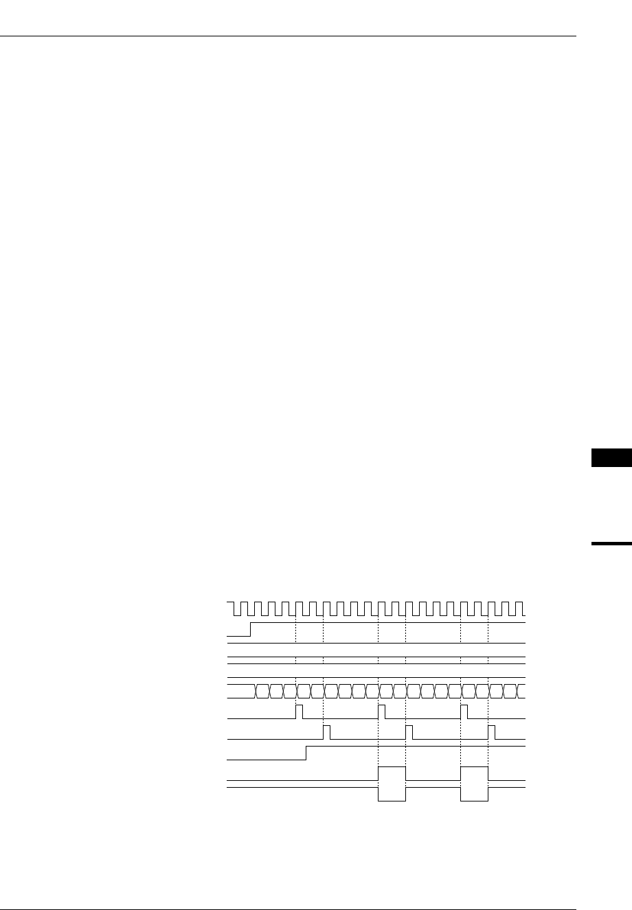
See Figure 4.3 for the waveforms.
Setting the output port
The TMx signal generated here can be output from the clock output pins (see Table 4.1), enabling a
programmable clock to be supplied to external devices.
After a cold start, the output pins are set for the I/O ports and set in input mode. The pins go into high-
impedance status.
When the pin function is switched to the timer output, the pin goes low if OUTINVx is set to "0" or goes high
if OUTINVx is set to "1".
Starting clock output
To output the TMx clock, write "1" to the clock output control bit PTMx. Clock output is stopped by writing
"0" to PTMx and goes to the off level according to the OUTINVx setting (low when OUTINVx = "0" or high
when OUTINVx = "1").
Timer 0 clock output control: PTM0 (D2) / 16-bit timer 0 control register (0x48186)
Timer 1 clock output control: PTM1 (D2) / 16-bit timer 1 control register (0x4818E)
Timer 2 clock output control: PTM2 (D2) / 16-bit timer 2 control register (0x48196)
Timer 3 clock output control: PTM3 (D2) / 16-bit timer 3 control register (0x4819E)
Timer 4 clock output control: PTM4 (D2) / 16-bit timer 4 control register (0x481A6)
Timer 5 clock output control: PTM5 (D2) / 16-bit timer 5 control register (0x481AE)
Figure 4.3 shows the waveform of the output signal.
Input clock
PRUNx
CRxA
CRxB
Counter value
Comparison match A signal
Comparison match B signal
PTMx
TMx output (when OUTINVx = "0")
TMx output (when OUTINVx = "1")
3
5
0 1 2 3 4 5 0 1 2 3 4 5 0 1 2 3 4 5 0 1
Figure 4.3 Waveform of 16-Bit Programmable Timer Output


