


4 PERIPHERAL CIRCUITS
S1C33L03 PRODUCT PART EPSON A-17
A-1
A-4
4.2 I/O Memory Map
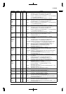
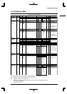
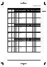
Table 4.2.1 I/O Memory Map
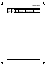
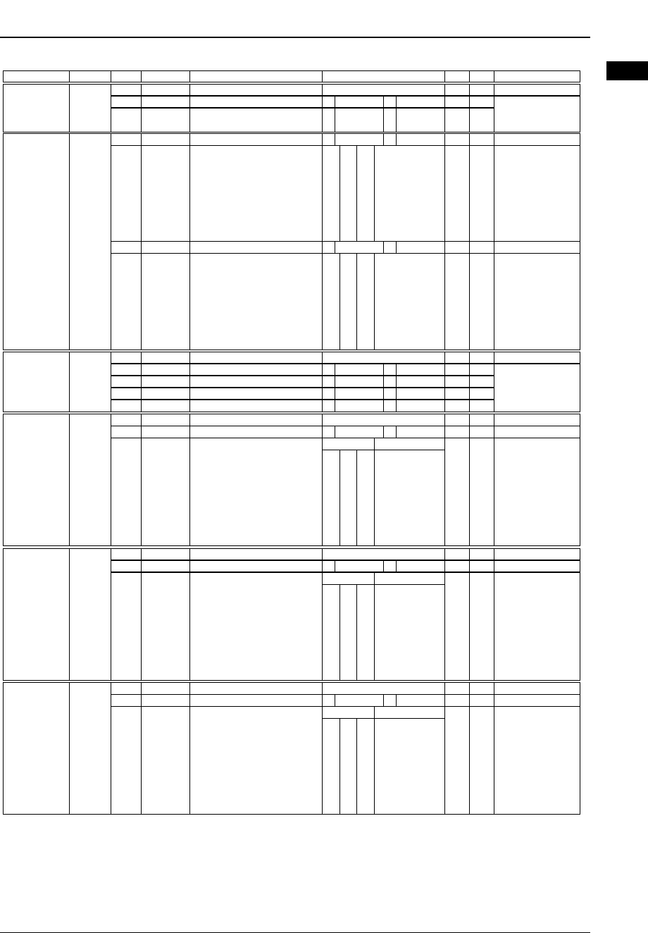
NameAddressRegister name Bit Function Setting Init. R/W Remarks
–
P8TPCK5
P8TPCK4
D7–2
D1
D0
reserved
8-bit timer 5 clock selection
8-bit timer 4 clock selection
–
0
0
–
R/W
R/W
0 when being read.
θ: selected by
Prescaler clock select
register (0x40181)
0040140
(B)
1 θ/1 0 Divided clk.
1 θ/1 0 Divided clk.
8-bit timer 4/5
clock select
register
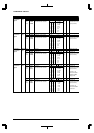
–
1 On 0 OffP8TON5
P8TS52
P8TS51
P8TS50
P8TON4
P8TS42
P8TS41
P8TS40
D7
D6
D5
D4
D3
D2
D1
D0
8-bit timer 5 clock control
8-bit timer 5
clock division ratio selection
8-bit timer 4 clock control
8-bit timer 4
clock division ratio selection
0
0
0
0
0
0
0
0
R/W
R/W
R/W
R/W
R/W
R/W
R/W
R/W
θ: selected by
Prescaler clock select
register (0x40181)
8-bit timer 5 can
generate the clock for
the serial I/F Ch.3.
θ: selected by
Prescaler clock select
register (0x40181)
8-bit timer 4 can
generate the clock for
the serial I/F Ch.2.
0040145
(B)
1
1
1
1
0
0
0
0
1
1
0
0
1
1
0
0
1
0
1
0
1
0
1
0
θ/256
θ/128
θ/64
θ/32
θ/16
θ/8
θ/4
θ/2
1 On 0 Off
1
1
1
1
0
0
0
0
1
1
0
0
1
1
0
0
1
0
1
0
1
0
1
0
θ/4096
θ/2048
θ/64
θ/32
θ/16
θ/8
θ/4
θ/2
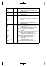
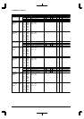
8-bit timer 4/5
clock control
register
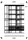
––
P8TPCK3
P8TPCK2
P8TPCK1
P8TPCK0
D7–4
D3
D2
D1
D0
reserved
8-bit timer 3 clock selection
8-bit timer 2 clock selection
8-bit timer 1 clock selection
8-bit timer 0 clock selection
–
0
0
0
0
–
R/W
R/W
R/W
R/W
0 when being read.
θ: selected by
Prescaler clock select
register (0x40181)
0040146
(B)
1 θ/1 0 Divided clk.
1 θ/1 0 Divided clk.
1 θ/1 0 Divided clk.
1 θ/1 0 Divided clk.
8-bit timer
clock select
register
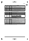
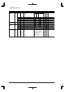
––
P16TON0
P16TS02
P16TS01
P16TS00
D7–4
D3
D2
D1
D0
reserved
16-bit timer 0 clock control
16-bit timer 0
clock division ratio selection
–
0
0
0
0
–
R/W
R/W
0 when being read.
θ: selected by
Prescaler clock select
register (0x40181)
16-bit timer 0 can be
used as a watchdog
timer.
0040147
(B)
1 On 0 Off
1
1
1
1
0
0
0
0
1
1
0
0
1
1
0
0
1
0
1
0
1
0
1
0
P16TS0[2:0] Division ratio
θ/4096
θ/1024
θ/256
θ/64
θ/16
θ/4
θ/2
θ/1
16-bit timer 0
clock control
register
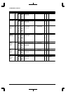
––
P16TON1
P16TS12
P16TS11
P16TS10
D7–4
D3
D2
D1
D0
reserved
16-bit timer 1 clock control
16-bit timer 1
clock division ratio selection
–
0
0
0
0
–
R/W
R/W
0 when being read.
θ: selected by
Prescaler clock select
register (0x40181)
0040148
(B)
1 On 0 Off
1
1
1
1
0
0
0
0
1
1
0
0
1
1
0
0
1
0
1
0
1
0
1
0
P16TS1[2:0] Division ratio
θ/4096
θ/1024
θ/256
θ/64
θ/16
θ/4
θ/2
θ/1
16-bit timer 1
clock control
register
––
P16TON2
P16TS22
P16TS21
P16TS20
D7–4
D3
D2
D1
D0
reserved
16-bit timer 2 clock control
16-bit timer 2
clock division ratio selection
–
0
0
0
0
–
R/W
R/W
0 when being read.
θ: selected by
Prescaler clock select
register (0x40181)
0040149
(B)
1 On 0 Off
1
1
1
1
0
0
0
0
1
1
0
0
1
1
0
0
1
0
1
0
1
0
1
0
P16TS2[2:0] Division ratio
θ/4096
θ/1024
θ/256
θ/64
θ/16
θ/4
θ/2
θ/1
16-bit timer 2
clock control
register
(B) in [Address] indicates an 8-bit register and (HW) indicates a 16-bit register.
The meaning of the symbols described in [Init.] are listed below:
0, 1: Initial values that are set at initial reset.
(However, the registers for the bus and input/output ports are not initialized at hot start.)
X: Not initialized at initial reset.
–: Not set in the circuit.