


4 PERIPHERAL CIRCUITS
A-24 EPSON S1C33L03 PRODUCT PART
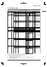
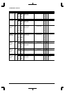
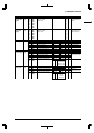
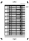
NameAddressRegister name Bit Function Setting Init. R/W Remarks
CLKDT1
CLKDT0
PSCON
–
CLKCHG
SOSC3
SOSC1
D7
D6
D5
D4–3
D2
D1
D0
System clock division ratio
selection
Prescaler On/Off control
reserved
CPU operating clock switch
High-speed (OSC3) oscillation On/Off
Low-speed (OSC1) oscillation On/Off
1 On 0 Off
1 OSC3 0 OSC1
1 On 0 Off
1 On 0 Off
0
0
1
0
1
1
1
R/W
R/W
–
R/W
R/W
R/W
Writing 1 not allowed.
0040180
(B)
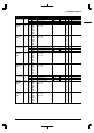
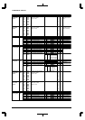
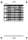
1
1
0
0
1
0
1
0
CLKDT[1:0] Division ratio
1/8
1/4
1/2
1/1
–
Power control
register
–
PSCDT0
D7–1
D0
reserved
Prescaler clock selection
0
0
–
R/W
0040181
(B)
–Prescaler clock
select register
1 OSC1 0 OSC3/PLL
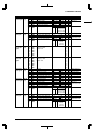
–
HLT2OP
8T1ON
–
PF1ON
D7–4
D3
D2
D1
D0
–
HALT clock option
OSC3-stabilize waiting function
reserved
OSC1 external output control
–
0
1
0
0
–
R/W
R/W
–
R/W
0 when being read.
Do not write 1.
0040190
(B)
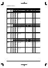
1 On 0 Off
1 Off 0 On
1 On 0 Off
–
–
Clock option
register
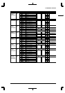
Writing 10010110 (0x96)
removes the write protection of
the power control register
(0x40180) and the clock option
register (0x40190).
Writing another value set the
write protection.
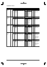
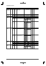
CLGP7
CLGP6
CLGP5
CLGP4
CLGP3
CLGP2
CLGP1
CLGP0
D7
D6
D5
D4
D3
D2
D1
D0
Power control register protect flag 0
0
0
0
0
0
0
0
R/W004019E
(B)
Power control
protect register