


VII LCD CONTROLLER BLOCK: LCD CONTROLLER
B-VII-2-30 EPSON S1C33L03 FUNCTION PART
Controlling the GPIO Pins
The pins described below can be used as general-purpose output (GPO) pins or general-purpose input/output
(GPIO) pins, through panel selection or other settings.
General-purpose output (GPO) pins
The FPDAT[3:0] signal output pins can be used as general-purpose output GPO[6:3] pins when a 4-bit LCD
panel (LDDW[1:0] (D[1:0])/0x39FFE1) = "00") is used. The GPO output control bits are listed in Table 2.19.
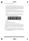
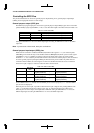
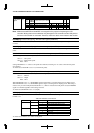
Table 2.19 GOP Control Bits
Pin name GPO signal name Output control bit
FPDAT0 GPO3 GPO3D (D3)/GPIO status/control register(0x39FFF9)
FPDAT1 GPO4 GPO4D (D4)/GPIO status/control register(0x39FFF9)
FPDAT2 GPO5 GPO5D (D5)/GPIO status/control register(0x39FFF9)
FPDAT3 GPO6 GPO6D (D6)/GPIO status/control register(0x39FFF9)
Setting the GPOxD bit to 1 drives the GPOx output high, and setting the GPOxD bit to 0 drives the GPOx
output low.
Note:In power-save or doze mode, these pins are fixed low.
General-purpose input/output (GPIO) pins
While the LCD controller is enabled (LCDCEN (D5)/LCDC mode register 2 = "1"), bus release requests
(#BUSREQ) from outside the chip can be disabled. When the BREQEN (D2)/LCDC system control register
(0x39FFFD) is set to "0" (default), bus release requests from outside will no longer be accepted while
LCDCEN = "1". As a result, the pins listed below will not be used for bus-release purposes, and can therefore
be used as general-purpose input/output (GPIO) pins. Because these pins are usable only while the LCD
controller remains enabled, the control registers in the LCD controller block must be used to control their
direction for input or output, as well as to read/write data to and from them.
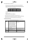
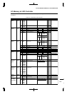
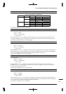
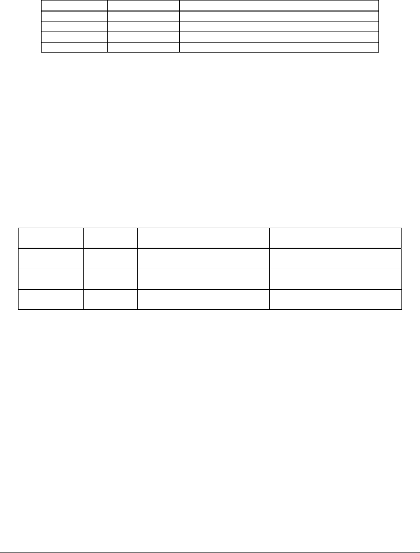
Table 2.20 GPIO Control Bits
Pin name
GPIO signal
name
I/O control bit I/O data
#BUSREQ/P34 GPIO0 GPIO0C (D0)/GPIO configuration
register(0x39FFF8)
GPIO0D (D0)/GPIO status/control
register(0x39FFF9)
#BUSACK/P35 GPIO1 GPIO1C (D1)/GPIO configuration
register(0x39FFF8)
GPIO1D (D1)/GPIO status/control
register(0x39FFF9)
#BUSGET/P31 GPIO2 GPIO2C (D2)/GPIO configuration
register(0x39FFF8)
GPIO2D (D2)/GPIO status/control
register(0x39FFF9)
Set the GPIOxC bits to "0" (default) when the GPIOx pins are used as input ports, or "1" when the GPIOx
pins are used as output ports.
When the pins are set for input, it possible to determine their input-voltage level by reading GPIOxD. The
value "1" is indicated when the input voltage is high, and "0" indicated when the input voltage is low.
When the pins are set for output, write output data to GPIOxD. Setting the GPIOxD bit to "1" drives the
GPIOx output high, and setting the GPIOxD bit to "0" drives the GPIOx output low.