II CORE BLOCK: BCU (Bus Control Unit)
S1C33L03 FUNCTION PART EPSON B-II-4-21
A-1
B-II
BCU
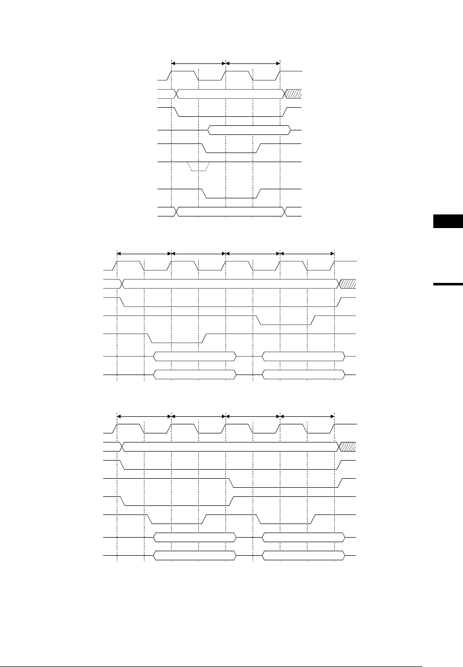
SRAM Write Cycles
Basic write cycle with no wait mode
BCLK
A[23:0]
#CExx
D[15:0]
#WRH/#WRL
#WAIT
#WR
#BSL/#BSH
addr
data
C1 C2
Figure 4.22 Half-word Write Cycle with No Wait
BCLK
A[23:0]
#CExx
#WRH
#WRL
D[15:8]
D[7:0]
C1 C2 C3 C4
addr
Undefined Valid
Valid Undefined
Figure 4.23 Byte Write Cycle with No Wait (A0 system, little endian)
BCLK
A[23:0]
#CExx
#BSH
#BSL
#WRL
D[15:8]
D[7:0]
C1 C2 C3 C4
addr
Undefined Valid
Valid Undefined
Figure 4.24 Byte Write Cycle with No Wait (#BSL system, little endian)


