


II CORE BLOCK: BCU (Bus Control Unit)
S1C33L03 FUNCTION PART EPSON B-II-4-39
A-1
B-II
BCU
A14DRA:Area 14 DRAM selection (D8) / Areas 14–13 set-up register (0x48122)
A13DRA:Area 13 DRAM selection (D7) / Areas 14–13 set-up register (0x48122)
A8DRA:Area 8 DRAM selection (D8) / Areas 8–7 set-up register (0x48128)
A7DRA:Area 7 DRAM selection (D7) / Areas 8–7 set-up register (0x48128)
Select the DRAM direct interface.
Write "1": DRAM is used
Write "0": DRAM is not used
Read: Valid
When DRAM is used by connecting it directly to the BCU, write "1" to this bit. The ordinary SRAM interface is
selected by writing "0" to the control bit.
The areas to which DRAM can be connected are areas 8 and 7 when the CEFUNC = "0", or areas 14 and 13 when
the bit = "1".
At cold start, these bits are set to "0" (DRAM not used). At hot start, the bits retain their status before being
initialized.
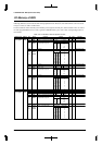
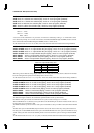
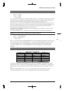
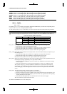
A10IR2–A10IR0: Area 10 internal ROM size selection (D[E:C]) / Areas 10–9 set-up register (0x48126)
Select an area 10 internal/emulation memory size.
Table 4.25 Area 10 Internal ROM Size
A10IR2 A10IR1 A10IR0 ROM size
000 16 KB
001 32 KB
010 64 KB
011 128 KB
100 256 KB
101 512 KB
110 1 MB
111 2 MB
At cold start, A10IR is set to "111" (2 MB). At hot start, A10IR retains its status before being initialized.
A10BW1–A10BW0: Burst read cycle wait control (D[A:9]) / Areas 10–9 set-up register (0x48126)
Set the number of wait cycles inserted during a burst read.
The values 0 to 3 written to the bits constitute the number of wait cycles inserted. The contents set here are applied
to both areas 10 and 9. The wait cycles set by AxxWT are inserted in the first read cycle of burst ROM and in the
burst ROM write cycle. For the burst ROM write cycle, the wait cycles set via the #WAIT pin can also be used.
At cold start, A10BW is set to "0" (no wait cycle). At hot start, A10BW retains its status before being initialized.