VI SDRAM CONTROLLER BLOCK: SDRAM INTERFACE
S1C33L03 FUNCTION PART EPSON B-VI-2-25
A-1
B-VI
SDRAM
A14SZ:Areas 14–13 device size selection (D6) / Areas 14–13 set-up register (0x48122)
A8SZ:Areas 8–7 device size selection (D6) / Areas 8–7 set-up register (0x48128)
Select the size of the device connected to each area.
Write "1": 8 bits
Write "0": 16 bits
Read: Valid
Set the device size of the area used for an SDRAM in the same manner as that specified for SDRSZ
(D6/0x39FFC9).
At cold start, these bits are set to "0" (16 bits). At hot start, these bits retain their status before being initialized.
A14WT2–A14WT0:Areas 14–13 wait control (D[2:0]) / Areas 14–13 set-up register (0x48122)
A8WT2–A8WT0:Areas 8–7 wait control (D[2:0]) / Areas 8–7 set-up register (0x48128)
A6WT2–A6WT0:Area 6 wait control (D[A:8]) / Areas 6–4 set-up register (0x4812A)
Set the number of wait cycles to be inserted when accessing the internal device.
The values 0 through 7 written to the control bits equal the number of wait cycles inserted.
Always make sure the number of wait cycles in area 6 (where the SDRAM controller is allocated) is 2 (A6WT =
"010"). With any other number of specified wait cycles, data may not be written normally to the SDRAM control
registers.
The number of wait cycles in areas used for SDRAMs should be set to 0 (A8WT/A14WT = "000").
At cold start, these bits are set to "111" (7 cycles). At hot start, the bits retain their status before being initialized.
A14DF1–A14DF0:
Areas 14–13 output disable delay time (D[5:4]) / Areas 14–13 set-up register (0x48122)
A8DF1–A8DF0: Areas 8–7 output disable delay time (D[5:4]) / Areas 8–7 set-up register (0x48128)
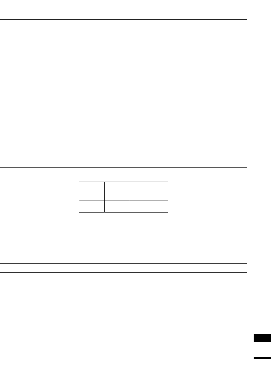
Set the output-disable delay time.
Table 2.13 Output Disable Delay Time
AxxDF1 AxxDF0 Delay time
113.5 cycles
102.5 cycles
011.5 cycles
000.5 cycles
If the system has an external memory device other than the SDRAM connected to it and accesses that memory
device and reads the SDRAM in succession, set the output disable delay time for the areas used for the SDRAM to
2.5 cycles (A8DF/A14DF = "10").
Otherwise, set the output disable delay time to 0.5 cycles (A8DF/A14DF = "00") in order to reduce the SDRAM
access time.
At cold start, these bits are set to "11" (3.5 cycles). At hot start, the bits retain their status before being initialized.
SWAITE: #WAIT enable (D0) / Bus control register (0x4812E)
Enable or disable wait cycle control.
Write "1": Enabled
Write "0": Disabled
Read: Valid
Because the SDRAM controller controls wait cycles internally in the IC, SWAITE must be set to "1".
At cold start, SWAITE is set to "0" (disabled). At hot start, SWAITE retains its status before being initialized.


