V DMA BLOCK: HSDMA (High-Speed DMA)
B-V-2-14 EPSON S1C33L03 FUNCTION PART
Single-address mode
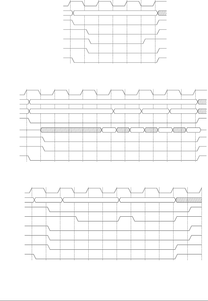
(1) SRAM
Example: When 2 (RD)/1 (WR) wait cycles are inserted
BCLK
A[23:0]
#CExx
#RD
#WRH/#WRL
#DMAACK
#DMAEND
addr
Figure 2.8 #DMAACK/#DMAEND Signal Output Timing (SRAM)
(2) Burst ROM
Example: When 4-consecutive-burst and 2-wait cycles are set during the first access
BCLK
A[23:2]
A[1:0]
#CE10(9)
D[15:0]
#RD
#DMAACK
#DMAEND
addr[23:2]
"11""10""01""00"
Figure 2.9 #DMAACK/#DMAEND Signal Output Timing (Burst ROM)
(3) DRAM
Example: Page mode, RAS: 1 cycle; CAS: 2 cycles; Precharge: 1 cycle
BCLK
A[11:0]
#RASx
#HCAS/
#LCAS
#RD
#WR
#DMAACK
#DMAEND
ROW COL #1 COL #2
Figure 2.10 #DMAACK/#DMAEND Signal Output Timing (DRAM)
Note: The single-address transfer method does not allow data transfer to/from the SDRAM.


