


III PERIPHERAL BLOCK: PRESCALER
S1C33L03 FUNCTION PART EPSON B-III-2-5
A-1
B-III
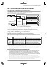
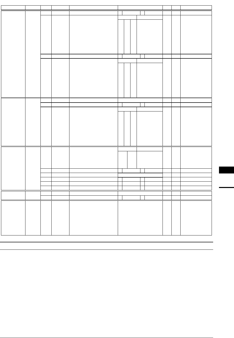
PSC
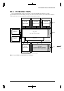
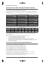
NameAddressRegister name Bit Function Setting Init. R/W Remarks
1 On 0 OffP8TON3
P8TS32
P8TS31
P8TS30
P8TON2
P8TS22
P8TS21
P8TS20
D7
D6
D5
D4
D3
D2
D1
D0
8-bit timer 3 clock control
8-bit timer 3
clock division ratio selection
8-bit timer 2 clock control
8-bit timer 2
clock division ratio selection
0
0
0
0
0
0
0
0
R/W
R/W
R/W
R/W
θ: selected by
Prescaler clock select
register (0x40181)
8-bit timer 3 can
generate the clock for
the serial I/F Ch.1.
θ: selected by
Prescaler clock select
register (0x40181)
8-bit timer 2 can
generate the clock for
the serial I/F Ch.0.
004014E
(B)
1
1
1
1
0
0
0
0
1
1
0
0
1
1
0
0
1
0
1
0
1
0
1
0
P8TS3[2:0] Division ratio
θ/256
θ/128
θ/64
θ/32
θ/16
θ/8
θ/4
θ/2
1 On 0 Off
1
1
1
1
0
0
0
0
1
1
0
0
1
1
0
0
1
0
1
0
1
0
1
0
P8TS2[2:0] Division ratio
θ/4096
θ/2048
θ/64
θ/32
θ/16
θ/8
θ/4
θ/2
8-bit timer 2/3
clock control
register
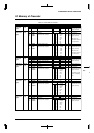
–
PSONAD
PSAD2
PSAD1
PSAD0
D7–4
D3
D2
D1
D0
reserved
A/D converter clock control
A/D converter clock division ratio
selection
–
0
0
0
0
–
R/W
R/W
0 when being read.
θ: selected by
Prescaler clock select
register (0x40181)
004014F
(B)
A/D clock
control register
1 On 0 Off
1
1
1
1
0
0
0
0
1
1
0
0
1
1
0
0
1
0
1
0
1
0
1
0
P8TS0[2:0] Division ratio
θ/256
θ/128
θ/64
θ/32
θ/16
θ/8
θ/4
θ/2
–
CLKDT1
CLKDT0
PSCON
–
CLKCHG
SOSC3
SOSC1
D7
D6
D5
D4–3
D2
D1
D0
System clock division ratio
selection
Prescaler On/Off control
reserved
CPU operating clock switch
High-speed (OSC3) oscillation On/Off
Low-speed (OSC1) oscillation On/Off
1 On 0 Off
1 OSC3 0 OSC1
1 On 0 Off
1 On 0 Off
0
0
1
0
1
1
1
R/W
R/W
–
R/W
R/W
R/W
Writing 1 not allowed.
0040180
(B)
1
1
0
0
1
0
1
0
CLKDT[1:0] Division ratio
1/8
1/4
1/2
1/1
–
Power control
register
–
PSCDT0
D7–1
D0
reserved
Prescaler clock selection
0
0
–
R/W
0040181
(B)
–Prescaler clock
select register
1 OSC1 0 OSC3/PLL
Writing 10010110 (0x96)
removes the write protection of
the power control register
(0x40180) and the clock option
register (0x40190).
Writing another value set the
write protection.
CLGP7
CLGP6
CLGP5
CLGP4
CLGP3
CLGP2
CLGP1
CLGP0
D7
D6
D5
D4
D3
D2
D1
D0
Power control register protect flag 0
0
0
0
0
0
0
0
R/W004019E
(B)
Power control
protect register
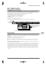
PSCON: Prescaler on/off control (D5) / Power control register (0x40180)
Turns the prescaler on or off.
Write "1": On
Write "0": Off
Read: Valid
The source clock is input to the prescaler by writing "1" to PSCON, thereby starting a dividing operation.
The prescaler is turned off by writing "0". If the peripheral circuits do not need to be operated, write "0" to this bit
to reduce current consumption. Since PSCON is protected against writing the same as SOSC1, SOSC3, CLKCHG
and CLKDT[1:0], CLGP[7:0] must be set to "0b10010110" before PSCON can be changed.
In addition, writing "0" (Off) to PSCON stops supplying the source clock to the prescaler and stops the peripheral
circuits that use the same clock (e.g., 16-bit programmable timers, 8-bit programmable timers, A/D converter,
serial interface, and ports). Therefore, do not turn off the prescaler when these peripheral circuits are used.
At initial reset, PSCON is set to "1" (On).