


II CORE BLOCK: BCU (Bus Control Unit)
S1C33L03 FUNCTION PART EPSON B-II-4-1
A-1
B-II
BCU
II-4 BCU (Bus Control Unit)
The BCU (Bus Control Unit) provides an interface for external devices and on-chip user logic block. The types
and sizes of memory and peripheral I/O devices can be set for each area of the memory map and can be controlled
directly by the BCU. This unit also supports a direct interface for DRAM and burst ROM. This chapter describes
how to control the external and internal system interface, and how it operates.
Note: The control registers of the external system interface shown in this chapter are mapped to the
internal 16-bit I/O area. Therefore, the addresses of these control registers are indicated by half-
word (16-bit) addresses unless otherwise specified. Note that the control registers can be
accessed in bytes, half-words, or words.
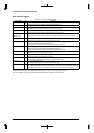
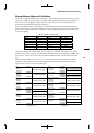
Pin Assignment for External System Interface
I/O Pin List
External I/O pins
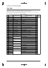
Table 4.1 lists the pins used for the external system interface.
Table 4.1 I/O Pin List
Pin name I/O Function
A[0]/#BSL O Address bus (A0) / Bus strobe (Low-byte)
A[10:1]/SDA[9:0]
O
Address bus (A1–A10) / SDRAM address bus (SDA0–SDA9)
A11
O
Address bus (A11)
A[13:12]/SDA[12:11]
O
Address bus (A12–A13) / SDRAM address bus (SDA11–SDA12)
A[15:14]/SDBA[1:0]
O
Address bus (A14–A15) / SDRAM bank select (SDBA0–SDBA1)
A[23:16] O Address bus (A16–A23)
D[15:0] I/O Data bus (D0–D15)
#CE10EX/#CE9&10EX O Area 10/(9&10) external memory chip enable
#CE9/#CE17/#CE17&18 O Area 9/17/(17&18) chip enable
#CE8/#RAS1/#CE14/#RAS3/#SDCE1 O Area 8/14 chip enable / DRAM Row strobe / SDRAM chip enable 1
#CE7/#RAS0/#CE13/#RAS2/#SDCE0 O Area 7/13 chip enable / DRAM Row strobe / SDRAM chip enable 0
#CE6/#CE7&8 O Area 6/(7&8) chip enable
#CE5/#CE15/#CE15&16 O Area 5/15/(15&16) chip enable
#CE4/#CE11/#CE11&12 O Area 4/11/(11&12) chip enable
#RD O Read signal
#EMEMRD O Read signal for area 3/10 emulation mode
#WRL/#WR/#WE O Write (Low-byte) / Write / DRAM write
#WRH/#BSH O Write (High-byte) / Bus strobe (High-byte)
#HCAS/#SDCAS O DRAM column address strobe (High-byte) / SDRAM column address strobe
#LCAS/#SDRAS O DRAM column address strobe (Low-byte) / SDRAM row address strobe
BCLK/SDCLK O Bus clock output / SDRAM operating clock
P35/#BUSACK/GPIO1 I/O I/O port / Bus request acknowledge / LCDC general-purpose input/output
P34/#BUSREQ/#CE6/GPIO0 I/O I/O port / Bus release request / Area 6 chip enable / LCDC general-purpose
input/output
P33/#DMAACK1/SIN3/SDA10 I/O I/O port / HSDMA Ch. 1 acknowledge output / Serial I/F Ch. 3 data input /
SDRAM address bus 10
P32/#DMAACK0/#SRDY3/HDQM I/O I/O port / HSDMA Ch. 0 acknowledge output / Serial I/F Ch. 3 ready signal output /
SDRAM data (high byte) input/output mask signal output
P31/#BUSGET/#GARD/GPIO2 I/O I/O port / Bus status monitor signal output / Area read signal output for GA /
LCDC general-purpose input/output
P30/#WAIT/#CE4&5 I/O I/O port / Wait cycle request / Areas 4&5 chip enable
P21/#DWE/#GAAS/#SDWE I/O I/O port / DRAM write (Low-byte) / Area address strobe output for GA / SDRAM write
P20/#DRD/SDCKE I/O I/O port / DRAM read / SDRAM clock enable
P15/EXCL4/#DMAEND0/#SCLK3/LDQM I/O I/O port / 16-bit timer 4 event counter input / HSDMA Ch. 0 end-of-transfer signal
output / Serial I/F Ch. 3 clock input/output / SDRAM data (low byte) input/output mask
signal output
#X2SPD I CPU - BCLK clock ratio
1: CPU clock = Bus clock, 0: CPU clock = Bus clock x 2
EA10MD[1:0] I Area 10 boot mode selection
11: External ROM, 10: Internal ROM