


8 ELECTRICAL CHARACTERISTICS
A-80 EPSON S1C33L03 PRODUCT PART
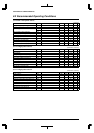
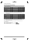
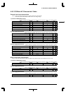
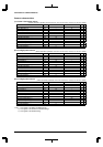
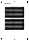
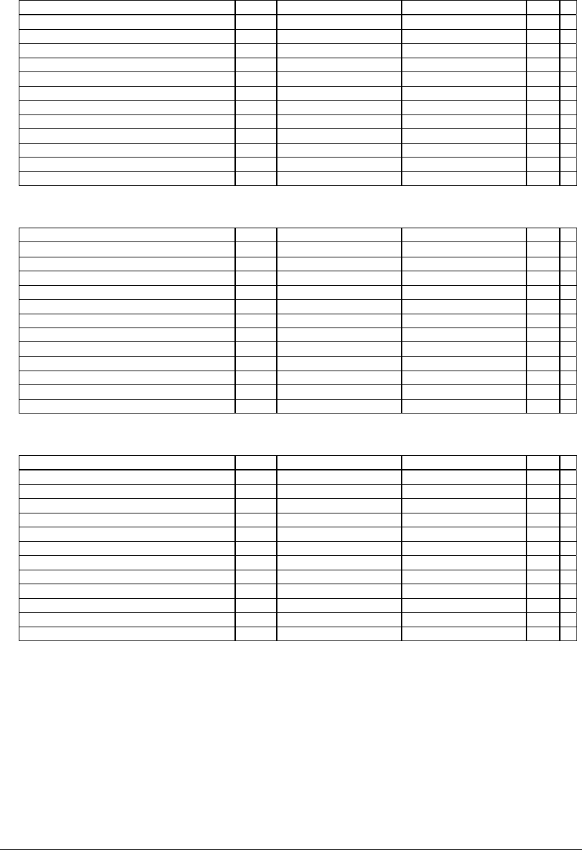
Common characteristics
1) 3.3 V/5.0 V dual power source
(Unless otherwise specified: VDDE=5.0V±0.5V, VDD=2.7V to 3.6V, VSS=0V, Ta=-40°C to +85°C)
Item Symbol Min. Max. Unit ∗
Address delay time tAD –8ns1
#CEx delay time (1) tCE1 –8ns
#CEx delay time (2) tCE2 –8ns
Wait setup time tWTS 15 – ns
Wait hold time tWTH 0–ns
Read signal delay time (1) tRDD1 8ns2
Read data setup time tRDS 12 ns
Read data hold time tRDH 0ns
Write signal delay time (1) tWRD1 8ns3
Write data delay time (1) tWDD1 10 ns
Write data delay time (2) tWDD2 010ns
Write data hold time tWDH 0ns
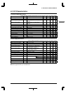
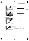
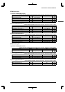
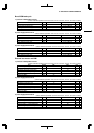
2) 3.3 V single power source
(Unless otherwise specified: VDDE=VDD=2.7V to 3.6V, VSS=0V, Ta=-40°C to +85°C)
Item Symbol Min. Max. Unit ∗
Address delay time tAD –10ns1
#CEx delay time (1) tCE1 –10ns
#CEx delay time (2) tCE2 –10ns
Wait setup time tWTS 15 – ns
Wait hold time tWTH 0–ns
Read signal delay time (1) tRDD1 10 ns 2
Read data setup time tRDS 15 ns
Read data hold time tRDH 0ns
Write signal delay time (1) tWRD1 10 ns 3
Write data delay time (1) tWDD1 10 ns
Write data delay time (2) tWDD2 010ns
Write data hold time tWDH 0ns
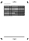
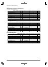
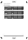
3) 2.0 V single power source
(Unless otherwise specified: VDDE=VDD=2.0V±0.2V, VSS=0V, Ta=-40°C to +85°C)
Item Symbol Min. Max. Unit ∗
Address delay time tAD –20ns1
#CEx delay time (1) tCE1 –20ns
#CEx delay time (2) tCE2 –20ns
Wait setup time tWTS 40 – ns
Wait hold time tWTH 0–ns
Read signal delay time (1) tRDD1 20 ns 2
Read data setup time tRDS 40 ns
Read data hold time tRDH 0ns
Write signal delay time (1) tWRD1 20 ns 3
Write data delay time (1) tWDD1 20 ns
Write data delay time (2) tWDD2 020ns
Write data hold time tWDH 0ns
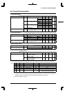
∗ note 1) This applies to the #BSH and #BSL timings.
2) This applies to the #GAAS and #GARD timings.
3) This applies to the #GAAS timing.