


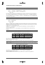
VI SDRAM CONTROLLER BLOCK: SDRAM INTERFACE
B-VI-2-24 EPSON S1C33L03 FUNCTION PART
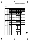
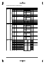
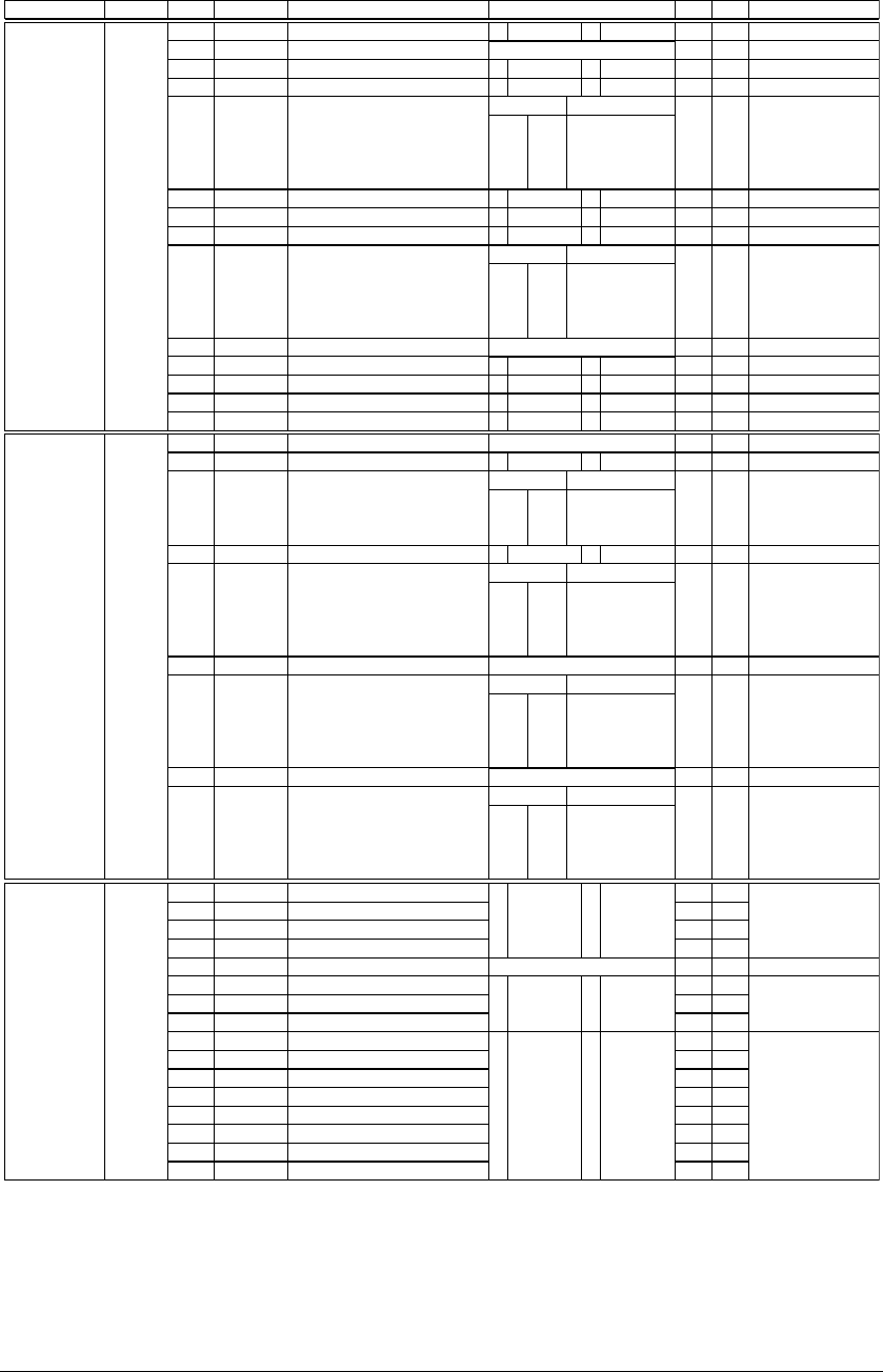
NameAddressRegister name Bit Function Setting Init. R/W Remarks
RBCLK
–
RBST8
REDO
RCA1
RCA0
RPC2
RPC1
RPC0
RRA1
RRA0
–
SBUSST
SEMAS
SEPD
SWAITE
DF
DE
DD
DC
DB
DA
D9
D8
D7
D6
D5
D4
D3
D2
D1
D0
BCLK output control
reserved
Burst ROM burst mode selection
DRAM page mode selection
Column address size selection
Refresh enable
Refresh method selection
Refresh RPC delay setup
Refresh RAS pulse width
selection
reserved
External interface method selection
External bus master setup
External power-down control
#WAIT enable
–
–
1 Fixed at H 0 Enabled
1
8-successive
0
4-successive
1 Enabled 0 Disabled
1 Self-refresh 0
CBR-refresh
1 2.0 0 1.0
1 #BSL 0 A0
1 Existing 0 Nonexistent
1 Enabled 0 Disabled
1 Enabled 0 Disabled
1 EDO 0 Fast page
0
0
0
0
0
0
0
0
0
0
0
0
0
0
0
0
R/W
–
R/W
R/W
R/W
R/W
R/W
R/W
R/W
–
R/W
R/W
R/W
R/W
Writing 1 not allowed.
Writing 1 not allowed.
004812E
(HW)
1
1
0
0
1
0
1
0
RCA[1:0] Size
11
10
9
8
1
1
0
0
1
0
1
0
RRA[1:0] Number of cycles
5
4
3
2
Bus control
register
1 Successive 0 Normal
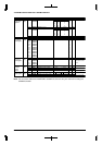
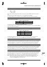
–
A3EEN
CEFUNC1
CEFUNC0
CRAS
RPRC1
RPRC0
–
CASC1
CASC0
–
RASC1
RASC0
DF–C
DB
DA
D9
D8
D7
D6
D5
D4
D3
D2
D1
D0
reserved
Area 3 emulation
#CE pin function selection
Successive RAS mode setup
DRAM
RAS precharge cycles selection
reserved
DRAM
CAS cycles selection
reserved
DRAM
RAS cycles selection
– –
1
0
0
0
0
0
–
0
0
–
0
0
–
R/W
R/W
R/W
R/W
–
R/W
–
R/W
0 when being read.
0 when being read.
0 when being read.
0048130
(HW)
1
0
0
x
1
0
CEFUNC[1:0]
#CE output
#CE7/8..#CE17/18
#CE6..#CE17
#CE4..#CE10
1
1
0
0
1
0
1
0
RPRC[1:0] Number of cycles
4
3
2
1
–
1
1
0
0
1
0
1
0
CASC[1:0] Number of cycles
4
3
2
1
–
1
1
0
0
1
0
1
0
RASC[1:0] Number of cycles
4
3
2
1
DRAM timing
set-up register
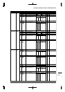
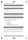
1
Internal ROM
0 Emulation
–
1 Internal
access
0 External
access
1 Internal
access
0 External
access
1 Big endian 0
Little endian
A18IO
A16IO
A14IO
A12IO
–
A8IO
A6IO
A5IO
A18EC
A16EC
A14EC
A12EC
A10EC
A8EC
A6EC
A5EC
DF
DE
DD
DC
DB
DA
D9
D8
D7
D6
D5
D4
D3
D2
D1
D0
Area 18, 17 internal/external access
Area 16, 15 internal/external access
Area 14, 13 internal/external access
Area 12, 11 internal/external access
reserved
Area 8, 7 internal/external
access
Area 6 internal/external
access
Area 5, 4 internal/external
access
Area 18, 17 endian control
Area 16, 15 endian control
Area 14, 13 endian control
Area 12, 11 endian control
Area 10, 9 endian control
Area 8, 7 endian control
Area 6 endian control
Area 5, 4 endian control
0
0
0
0
0
0
0
0
0
0
0
0
0
0
0
0
R/W
R/W
R/W
R/W
–
R/W
R/W
R/W
R/W
R/W
R/W
R/W
R/W
R/W
R/W
R/W
0 when being read.
0048132
(HW)
Access control
register