VI SDRAM CONTROLLER BLOCK: SDRAM INTERFACE
S1C33L03 FUNCTION PART EPSON B-VI-2-1
A-1
B-VI
SDRAM
VI-2 SDRAM INTERFACE
The SDRAM controller allows up to 32MB of SDRAM to be connected directly to areas 7 and 8 or areas 13 and
14. This chapter describes how to control the SDRAM interface, and how it operates. For the conditions and
parameters used to configure the external bus except for the SDRAM interface, refer to Chapter II-4, "BCU (Bus
Control Unit)".
Outline of SDRAM Interface
The following shows the main features and specifications of the SDRAM interface.
•Supports 8 or 16-bit SDRAM.
•Two SDRAM areas (areas 7 and 8 or areas 13 and 14)
The following SDRAM configuration (maximum) is possible, connected directly to each area.
- 16M × 16 bits × 1 chip
- 8M × 16 bits × 2 chips
- 32M × 8 bits × 1 chip
- 16M × 8 bits × 2 chips
•Supports 2 or 4-bank SDRAM (BA1 and BA0 outputs).
Row address range: 2K (A10–A0), 4K (A11–A0), or 8K (A12–A0)
Column address range: 256 (A7–A0), 512 (A8–A0), or 1K (A9–A0)
•Incorporates a programmable 12-bit auto refresh counter.
The SDRAM can be refreshed as necessary, irrespective of the clock frequency used.
•Intelligent self-refresh mode for low-power operation
•Two power-up options:
- Precharge → Refresh → Mode Register Set
- Precharge → Mode Register Set → Refresh
•CAS latency: 2
•Burst length: Can be set to 1, 2, 4, or 8 words.
SDRAM Controller Block Diagram
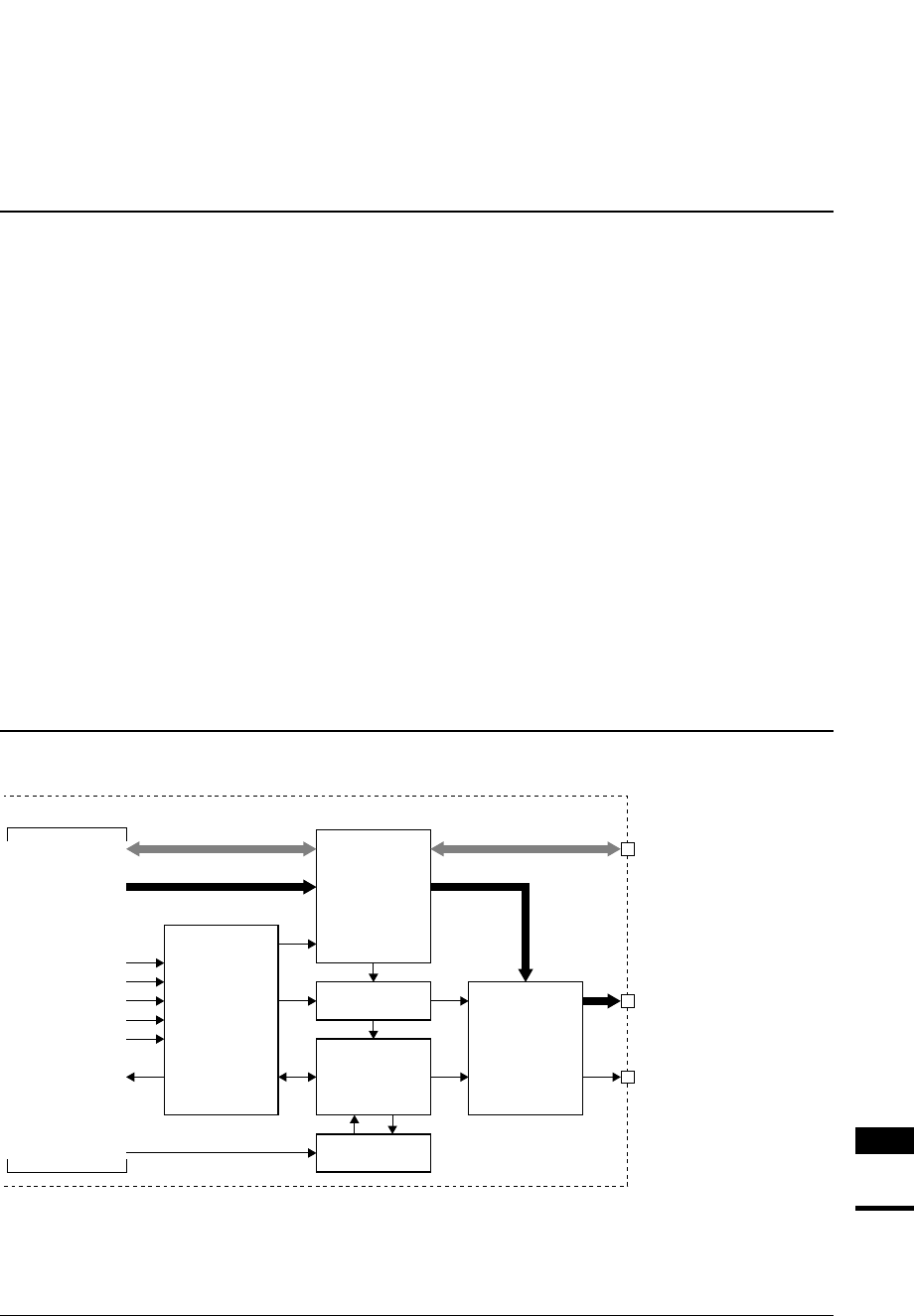
Figure 2.1 shows the block diagram of the SDRAM controller. Note that the signals described in the figure are
internal use, not external signals.
Bus
multiplex
Control
registers
SDRAM state
control
Address[23:0]
Bus Size
Data[15:0]
addr[23:0]
D[15:0]
SDA[12:11], SDA[9:0]
SDA10, SDCKE, #SDCE0/1
#SDCAS, #SDRAS
#SDWE, HDQM, LDQM
Bus command
decoder
SDRAM
command
decoder
Refresh
counter
Bus Mode
Internal #CE6
Internal #CE7/13
Internal #CE8/14
Internal #WAIT
OSC3 clock
User logic signals
Figure 2.1 SDRAM Controller Block Diagram


