


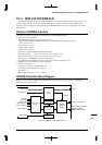

VI SDRAM CONTROLLER BLOCK: SDRAM INTERFACE
S1C33L03 FUNCTION PART EPSON B-VI-2-7
A-1
B-VI
SDRAM
Memory Configuration
Use the registers described below to select the area in which SDRAMs are connected and the chip enable
output pin to be used for SDRAMs.
Selecting areas
Area 7 or 13: SDRAR0 (D7)/SDRAM area configuration register (0x39FFC0)
Area 8 or 14: SDRAR1 (D6)/SDRAM area configuration register (0x39FFC0)
Writing "1" to SDRARx sets the corresponding area for SDRAM use. When SDRARx = "0" (default), the
area is used for devices other than SDRAM that are controlled only by the BCU.
Selecting chip enable
#SDCE0(#CE7/13): SDRPC0 (D3)/SDRAM area configuration register (0x39FFC0)
#SDCE1(#CE8/14): SDRPC1 (D2)/SDRAM area configuration register (0x39FFC0)
Writing "1" to SDRPCx sets the corresponding pin for SDRAM chip enable output. When SDRPCx = "0"
(default), the pin is used for devices other than SDRAM that are controlled only by the BCU.
Although #SDCE0 and #SDCE1 are assigned to the #CE7 and #CE8 pins, respectively, they are not
necessarily fixed to either area. For example, even when using area 7 or 13 for SDRAMs, the chip enable
used for the SDRAM can be #SDCE1 (#CE8/14).
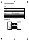
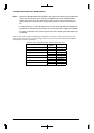
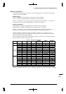
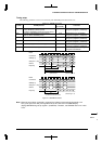
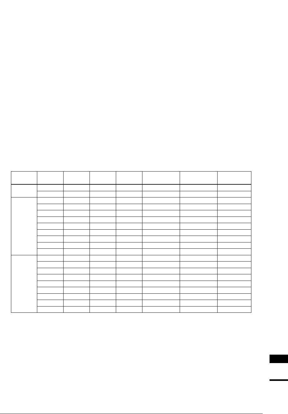
Table 2.5 lists the chip enable address ranges and the SDRAM sizes that can be connected when the area(s)
and chip enable are selected according to the above.
Table 2.5 Chip Enable Configuration
CEFUNC SDRAR0 SDRAR1 SDRPC0 SDRPC1
#SDCE0
address range
#SDCE1
address range
SDRAM size
(16-bit)
00XX N/A N/A 0
XX
XX00 N/A N/A 0
1010Area 7 N/A 2MB
1001 N/A Area 72MB
1011Area 7 N/A 2MB
0110Area 8 N/A 2MB
0101 N/A Area 82MB
0111 N/A Area 82MB
1110Area 7&8N/A 4MB
1101 N/AArea 7&84MB
00
(default)
1111Area 7Area 82MB x 2
1010Area 13 N/A 16MB
1001 N/A Area 1316MB
1011Area 13 N/A 16MB
0110Area 14 N/A 16MB
0101 N/A Area 1416MB
0111 N/A Area 1416MB
1110Area 13&14N/A 32MB
1101 N/AArea 13&1432MB
01
10
11
1111Area 13Area 1416MB x 2
Area 7 = 0x400000–0x5FFFFF, Area 8 = 0x600000–0x7FFFFF, Area 7&8 = 0x400000–0x7FFFFF
Area 13 = 0x2000000–0x2FFFFFF, Area 14 = 0x3000000–0x3FFFFFF, Area 13&14 = 0x2000000–0x3FFFFFF